Debugging method and debugging system of SOC chip

A debugging method and technology for debugging systems, which are applied in the detection of faulty computer hardware, instruments, and functional testing, etc., and can solve problems such as expensive kits

Active Publication Date: 2012-06-13
HISENSE VISUAL TECH CO LTD
View PDF2 Cites 15 Cited by
  • Summary
  • Abstract
  • Description
  • Claims
  • Application Information

AI Technical Summary

Problems solved by technology

Common debugging interfaces include USB (Universal Serial BUS, Universal Serial Bus), JTAG (Joint Test Action Group, Joint Test Action Group), etc., but these debugging methods need to purchase a set of debugging tools and debugging development environment. tend to be more expensive

Method used


Image

  • Debugging method and debugging system of SOC chip
  • Debugging method and debugging system of SOC chip
  • Debugging method and debugging system of SOC chip

Examples


Embodiment Construction

[0017] In order to understand the above-mentioned purpose, features and advantages of the present invention more clearly, the present invention will be further described in detail below in conjunction with the accompanying drawings and specific embodiments.

[0018] In the following description, many specific details are set forth in order to fully understand the present invention, but the present invention can also be implemented in other ways different from those described here, therefore, the present invention is not limited to the specific embodiments disclosed below limit.

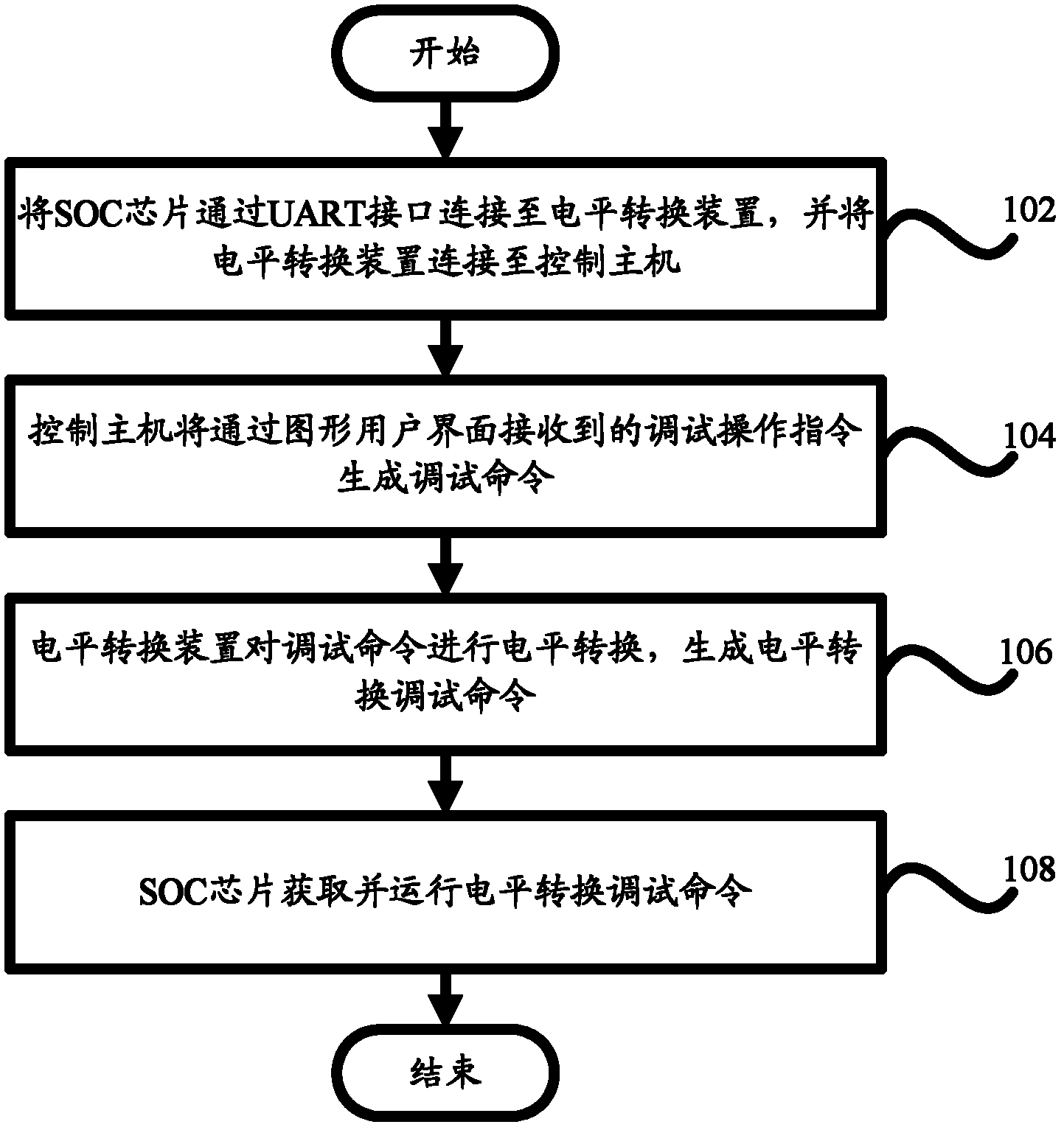
[0019] figure 1 A flow chart of a debugging method for an SOC chip according to an embodiment of the present invention is shown.

[0020] like figure 1 As shown, the debugging method of the SOC chip according to the embodiment of the present invention includes: step 102, the SOC chip is connected to the level conversion device through the UART interface, and the level conversion device is connected ...


PUM


Abstract

The invention provides a debugging method of an SOC chip, which includes the following steps: step 102, connecting the SOC chip to a level switch device through a universal asynchronous receiver / transmitter (UART) port and connecting the level switch device to a control main machine; step 104, generating debugging operation indications received through the picture user interface into debugging orders through the control machine; step 106, conducting level switch on the debugging orders through the level switch device to generate level switch debugging orders; and step 108, obtaining and operating level switch debugging orders through the SOC chip. Correspondingly, a debugging system of the SOC chip is further provided. By means of the technical scheme, debugging of the SOC chip can be achieved through the UART port, and cost in the debugging process is greatly reduced. Simultaneously, the picture user interface is adopted to receive operation indications and generate debugging orders to achieve batch processing of the SOC chip and improve debugging efficiency.

Description

technical field [0001] The invention relates to a debugging technology of an SOC chip, in particular to a debugging method and a debugging system of an SOC chip. Background technique [0002] SOC (System-on-a-chip, system on chip) video processing chip is a collection of many IP resources, including CPU, VIDEO DECODER and many video processing modules. After the overall architecture of the chip is built, a unified debugging method is required to debug all the modules and system software in the chip. Common debugging interfaces include USB (Universal Serial BUS, Universal Serial Bus), JTAG (Joint Test Action Group, Joint Test Action Group), etc., but these debugging methods need to purchase a set of debugging tools and a debugging development environment. Tends to be more expensive. However, SOC chips generally have a hardware UART (Universal Asynchronous Receiver / Transmitter, Universal Asynchronous Receiver / Transmitter) interface, and the debugging instructions are transmi...

Claims


Application Information

Patent Timeline
Patent Type & Authority Applications(China)
IPC IPC(8): G06F11/26G06F13/20
Inventor 徐卫
Owner HISENSE VISUAL TECH CO LTD
Why Eureka
Try Eureka