Welding spot defect identifying method

A solder joint and defect technology, applied in the field of microelectronic packaging and assembly, can solve problems such as easy to fall into local optimal solution, slow convergence of neural network, etc.

Inactive Publication Date: 2012-06-20
GUILIN UNIV OF ELECTRONIC TECH
View PDF2 Cites 28 Cited by
  • Summary
  • Abstract
  • Description
  • Claims
  • Application Information

AI Technical Summary

Problems solved by technology

At present, for the defect identification of solder joints, it is mainly through feature extraction of the collected image information of solder joints, and then using methods such as threshold discrimination, fuzzy reasoning and neural networks to identify solder joint defects. However, the neural network has a convergence Slow and easy to fall into local optimal solution and other defects

Method used


Image

  • Welding spot defect identifying method
  • Welding spot defect identifying method
  • Welding spot defect identifying method

Examples


Embodiment Construction

[0061] The present invention will be described in detail below with reference to the accompanying drawings.

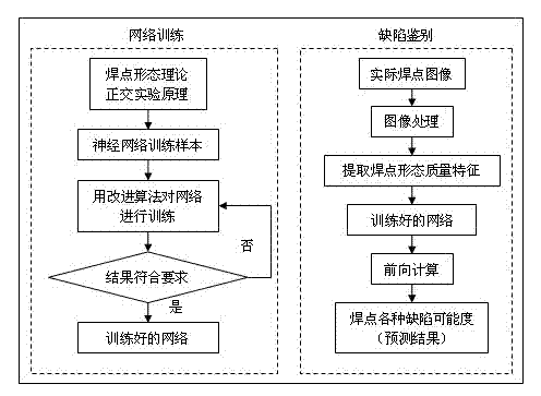
[0062] See figure 1 . The invention is divided into two parts: network training and defect identification.

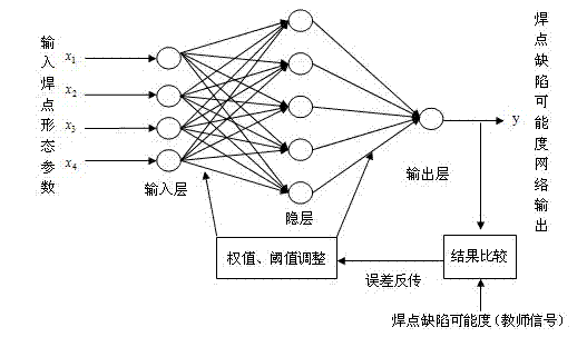
[0063] The network training includes 1), based on the shape theory of solder joints, and according to the principle of orthogonal experiment, to obtain the samples used for training the artificial neural network; 2), to train the artificial neural network with the improved neural network algorithm, and to obtain A network of various defect possibilities for solder joints. Defect identification includes image processing of actual solder joints, extracting morphological quality features as the input of the trained artificial neural network, and using the trained network for forward calculation to realize the identification of solder joint defects.

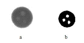
[0064] Taking BGA solder joints with a solder ball diameter of 0.75mm and a solder ball pitch of 1.27mm as an examp...


PUM


Abstract

The invention provides a welding spot defect identifying method which comprises a step of performing characteristic extraction on the acquired welding spot image information and a step of identifying the welding spot defect according to the ways of identifying, fuzzy inference, neutral network according to the characteristics and the like, and specifically comprises the following steps of: 1) obtaining a sample for training an artificial neural network according to the principle of an orthogonal test based on the welding spot shape theory; 2) training the artificial neural network by use of an improved neural network algorithm to obtain a network for predicting the possibility of various defects of the welding spots; and 3) performing image processing on the actual welding spot, extracting the shape quality characteristic as the input of the trained artificial neural network, and performing forward calculation by use of the trained network to realize identification of the welding spot defect. In the invention, as the BP neural network is improved and the genetic algorithm is introduced into the neural network algorithm training, the defects of slow convergence, easy trap in local optimal solution and the like of the neural network are solved, and the network performance is improved to some degree so as to realize defect identification of complicated welding spots.

Description

technical field [0001] The invention relates to microelectronic packaging and assembly technology, in particular to a method for identifying solder joint defects. Background technique [0002] Solder joint defect identification technology is to rely on advanced optical or electromagnetic technology to collect image information of solder joints without destroying the actual solder joint shape, process the collected image information of solder joints, and extract the information that affects the shape of solder joints. Some important features of these information, and various analysis, processing, differentiation and identification of this information, to confirm its solder joint defects. At present, for the defect identification of solder joints, it is mainly through feature extraction of the collected image information of solder joints, and then using methods such as threshold discrimination, fuzzy reasoning and neural networks to identify solder joint defects. However, the ...

Claims


Application Information

Patent Timeline
Patent Type & Authority Applications(China)
IPC IPC(8): G06K9/62G06N3/02
Inventor 周德俭李春泉吴兆华黄春跃陈小勇
Owner GUILIN UNIV OF ELECTRONIC TECH
Why Eureka
Try Eureka