Eureka AIR delivers breakthrough ideas for toughest innovation challenges, trusted by R&D personnel around the world.

Manufacturing process for circuit board with long and short gold fingers

A circuit board manufacturing and gold finger technology, which is applied in the directions of printed circuit components, electrical connection printed components, and printed component electrical connection formation, etc., can solve the problems of long production cycle, complex gold finger process, low product reliability, etc. The effect of avoiding residues, reducing the area of ​​the physical connection structure, and shortening the production cycle

Inactive Publication Date: 2012-06-20
SHENZHEN WUZHU TECH +1
View PDF4 Cites 3 Cited by
  • Summary
  • Abstract
  • Description
  • Claims
  • Application Information

AI Technical Summary

Problems solved by technology

[0012] Aiming at the problems in the prior art of printed circuit board gold fingers with long and short gold fingers, which have complex process, long production cycle and low product reliability, the present invention provides a long and short gold finger with simple gold finger process, short production cycle and high reliability. circuit board manufacturing process

Method used


Image

  • Manufacturing process for circuit board with long and short gold fingers
  • Manufacturing process for circuit board with long and short gold fingers
  • Manufacturing process for circuit board with long and short gold fingers

Examples


Embodiment Construction

[0029] The specific implementation of the manufacturing process of the long and short gold finger circuit board of the present invention will be described in detail below with reference to the accompanying drawings.

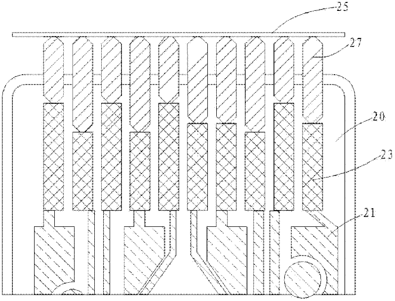
[0030] See figure 2 , Is a schematic diagram of the planar structure of a circuit board in the process of the present invention. The circuit board 2 is a rigid printed circuit board with long and short golden finger structures. The circuit board 2 includes a substrate 20, a plurality of conductive patterns 21 formed on the surface of the substrate 20, a plurality of gold fingers 23, a frame 25 and gold-plated leads 27.

[0031] The substrate 20 is a carrier substrate processed from an insulating resin material for carrying the conductive pattern 21, a plurality of gold fingers 23, a frame 25, and a gold-plated lead 27 on its surface. The gold-plated lead 27 is electrically connected to the plurality of gold fingers 23 correspondingly. At the same time, the gold-pla...


PUM


Abstract

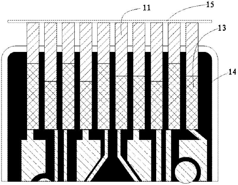
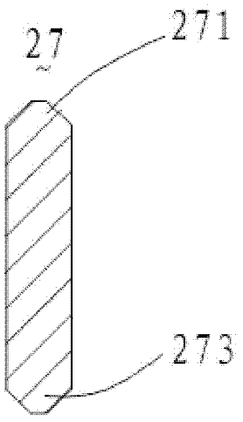
The invention relates to a manufacturing process for a circuit board with long and short gold fingers, which comprises the following steps: supplying a base plate; arranging a plurality of gold finger patterns on the surface of the base plate; arranging a gold-plated lead with tip structures on the surface of the base plate; correspondingly and electrically connecting the tip structures of the gold-plated lead with the gold finger patterns; performing gold-plating treatment on the gold finger patterns so as to form the gold fingers; and tearing off and removing the gold-plated lead, thereby separating the tip structures of the gold-plated lead from the gold fingers. According to the manufacturing process for the circuit board provided by the invention, the tip structures are arranged at the end parts of the gold-plated lead, so that the gold-plated lead and the gold fingers are electrically connected while an area of a physical connecting structure between the gold-plated lead and the gold fingers is greatly reduced. When a test is finished, an operator can easily remove the gold-plated lead in the manner of pulling and tearing by hand, and the gold-plated lead is prevented from being remained, so that the change in electric properties of the gold fingers caused by the remained gold-plated lead is avoided, the short circuit risk is eliminated and the reliability of products is increased.

Description

Technical field [0001] The invention relates to a circuit board manufacturing process, in particular to a circuit board manufacturing process with long and short golden fingers. Background technique [0002] Printed Circuit Board (PCB) is the basis of almost any electronic product and appears in almost every electronic device or product. Generally speaking, if there are electronic functional modules in a certain device or product, they are also installed on the surface of PCBs of different sizes. It can be seen that the optimization of printed circuit boards and their manufacturing processes is becoming more and more important with the market demand of printed circuit boards. [0003] With the development of the current electronic product field, the design of each electronic function module is more inclined to support the plug-and-pull mode, that is, the electronic function module can be connected or disconnected with the device without cutting off the power, because the electroni...

Claims


Application Information

Patent Timeline
IPC IPC(8): H05K3/40H05K1/11
Inventor 徐学军
Owner SHENZHEN WUZHU TECH
Why Eureka
Eureka Blog
Learn More