
Eureka
For R&D, Eureka makes reading and utilizing patents & technical documents easy.
Eureka AIR
Designed for self-driven R&D workflows. Generate viable solutions, solve complex R&D challenges, empower your innovation with AI.

Eureka Materials
Designed for material experts only. Revolutionize your material R&D, from search, analyze, to developing new materials.

TechResearch
Generate reliable direction feasibility study reports for your R&D in just a few steps.

TechSeek
Discover and master advanced knowledge NOW. Basics, ideas, possibilities, all at once.

TechMind
As an expert in R&D Theories, TechMind can generates customized viable solutions instantly.

TechRisk
Analyze your overall solution with one click, know your potential R&D risks in advance.

TechMonitor
Get weekly tech updates, stay abreast of the latest tech innovations and key insights.
Solder resist manufacturing method of thick copper plate
A production method and technology for thick copper plates, which are used in the solder mask production of thick copper plates. In the field of solder mask production of 4OZ PCB boards, it can solve the problems of inconsistent thickness of line and corner ink, and achieve uniformity and consistency, and increase the thickness. Effect
- Summary
- Abstract
- Description
- Claims
- Application Information
AI Technical Summary
Problems solved by technology
Method used
Image

Examples
Embodiment Construction
[0022] To illustrate the idea and purpose of the present invention, the present invention will be further described below in conjunction with the accompanying drawings and specific embodiments.
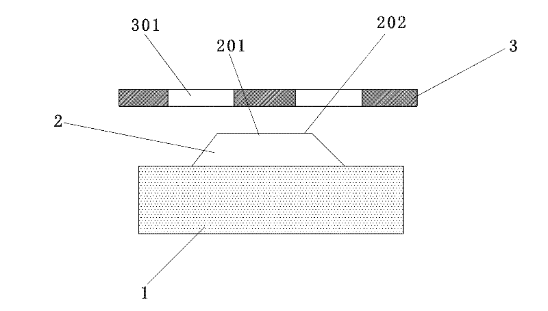
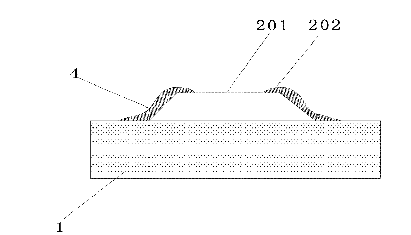
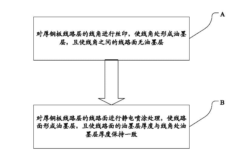
[0023] The present invention provides a method for making thick copper plates for solder resist. By first performing wire corner silk screen printing and then performing circuit surface silk printing, it solves the problem of the current thick copper plate solder resist manufacturing using secondary silk printing or spraying. The problem of inconsistency between the thickness of the surface ink and the thickness of the line angle ink.
[0024] See figure 1 , figure 2 As shown, figure 1 It is a schematic diagram of the cross-sectional structure of the circuit board of the present invention for line corner silk screen printing through the screen; figure 2 It is a schematic diagram of the screen printing effect of the line angle of the circuit board of the present invention. The thick coppe...
PUM
 Abstract
Description
Claims
Application Information
 - R&D Engineer
- R&D Manager
- IP Professional
- Industry Leading Data Capabilities
- Powerful AI technology
- Patent DNA Extraction
Browse by: Latest US Patents, China's latest patents, Technical Efficacy Thesaurus, Application Domain, Technology Topic, Popular Technical Reports.
© 2024 PatSnap. All rights reserved.Legal|Privacy policy|Modern Slavery Act Transparency Statement|Sitemap|About US| Contact US: help@patsnap.com