Method, system and circuit board for making circuit board bumps

A technology of circuit boards and bumps, applied in printed circuits, printed circuit manufacturing, printed circuit components, etc., can solve problems such as cumbersome production process, complicated operation, and affecting the accuracy of bumps

Active Publication Date: 2015-12-16
NEW FOUNDER HLDG DEV LLC
View PDF6 Cites 0 Cited by
  • Summary
  • Abstract
  • Description
  • Claims
  • Application Information

AI Technical Summary

Problems solved by technology

The inventors of the present invention have found that, in view of the current conventional bump manufacturing method, two stripping processes need to be carried out during the fabrication process: respectively stripping the temporary film when making the circuit and stripping the temporary film when making the bump, It is also necessary to carry out the alignment process of bump graphics production, that is, to calibrate the position with the corresponding line gasket. The production process is cumbersome and the operation is complicated, which affects the accuracy of bumps.

Method used


Image

  • Method, system and circuit board for making circuit board bumps
  • Method, system and circuit board for making circuit board bumps
  • Method, system and circuit board for making circuit board bumps

Examples


Embodiment Construction

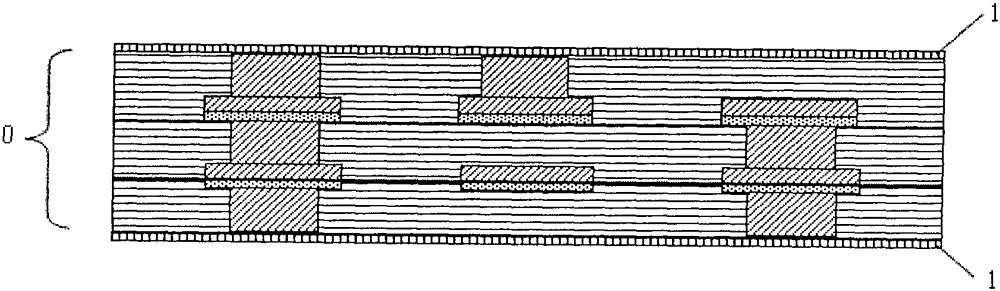
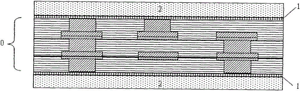
[0030] Embodiments of the present invention provide a method, system, and circuit board for making bumps on a circuit board. After making the circuit, the bump is directly made, and after the bump is made, the temporary film when making the circuit and the temporary film when making the bump are removed together. Temporary film, since the film is only removed once, it can reduce the probability of production defects due to unclean film removal. At the same time, because the temporary film during the production of the circuit is not removed when making the bumps, the production of bumps is omitted. During the alignment process, the displacement tolerance of the bump is the tolerance when making the circuit, which improves the manufacturing accuracy of the bump on the circuit board.

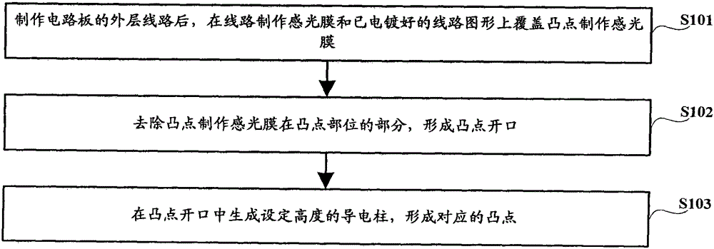
[0031] The invention provides a method for making circuit board bumps, which is characterized in that, comprising:

[0032] After making the outer circuit of the circuit board, make a temporary fil...


PUM


Abstract

The invention discloses a method and a system for manufacturing bumps on circuit boards and a circuit board utilizing the same, which relate to the field of manufacturing of circuit boards. The method for manufacturing bumps on the circuit boards includes: directly manufacturing bumps after circuits are manufactured and removing temporary films used in circuit manufacturing and removing temporary films used in bump manufacturing. Probability of production defects due to incomplete film removal can be decreased by removing films once, and meanwhile, during bump manufacturing, the temporary films used during circuit manufacturing is not removed, so that alignment during bump manufacturing is omitted, displacement tolerance of the bumps is the tolerance during circuit manufacturing, and manufacturing precision of the bumps of the circuit boards is increased.

Description

technical field [0001] The invention relates to the field of circuit board production, in particular to a method, system and circuit board for producing circuit board bumps. Background technique [0002] With the development of electronic products in the direction of lightness, thinness, shortness, smallness and multiple functions, new requirements are constantly put forward for electronic packaging. To meet this need, flip-chip (Flip-Chip) technology is Performance, high I / O pin count, package size reduction and other advantages are increasingly widely used. Flip-chip technology adopts chip-to-substrate bonded packaging. The packaging method is that the front of the chip faces the substrate without wire bonding. Compared with traditional wire connection and carrier tape connection, the obvious advantages of flip-chip technology include: the highest packaging density, It has good electrical and thermal performance, good reliability, and low cost. Therefore, flip chip techn...

Claims


Application Information

Patent Timeline
Patent Type & Authority Patents(China)
IPC IPC(8): H05K3/34H05K3/00H05K1/11
Inventor 苏新虹朱兴华
Owner NEW FOUNDER HLDG DEV LLC
Why Eureka
Try Eureka