Manufacturing method of circuit boards

A manufacturing method and circuit board technology, which are applied in the direction of electronic circuit testing, electrical connection formation of printed components, etc., can solve problems such as loss of circuit boards, difficult to accurately conduct through holes of circuit boards, etc., and achieve accurate conduction, Avoid the effects of destructive testing

Active Publication Date: 2014-02-05
HONGQISHENG PRECISION ELECTRONICS (QINHUANGDAO) CO LTD +1
View PDF5 Cites 0 Cited by
  • Summary
  • Abstract
  • Description
  • Claims
  • Application Information

AI Technical Summary

Problems solved by technology

In this way, the destructive test of the circuit board not only loses the tested circuit board, but also makes it difficult to accurately obtain the conductivity of the via hole of each circuit board.

Method used


Image

  • Manufacturing method of circuit boards
  • Manufacturing method of circuit boards
  • Manufacturing method of circuit boards

Examples


Embodiment Construction

[0072] The manufacturing method of the circuit board provided by the technical solution will be further described in detail below in conjunction with multiple drawings and embodiments.

[0073] The circuit board manufacturing method provided by the embodiment of the technical solution includes the following steps:

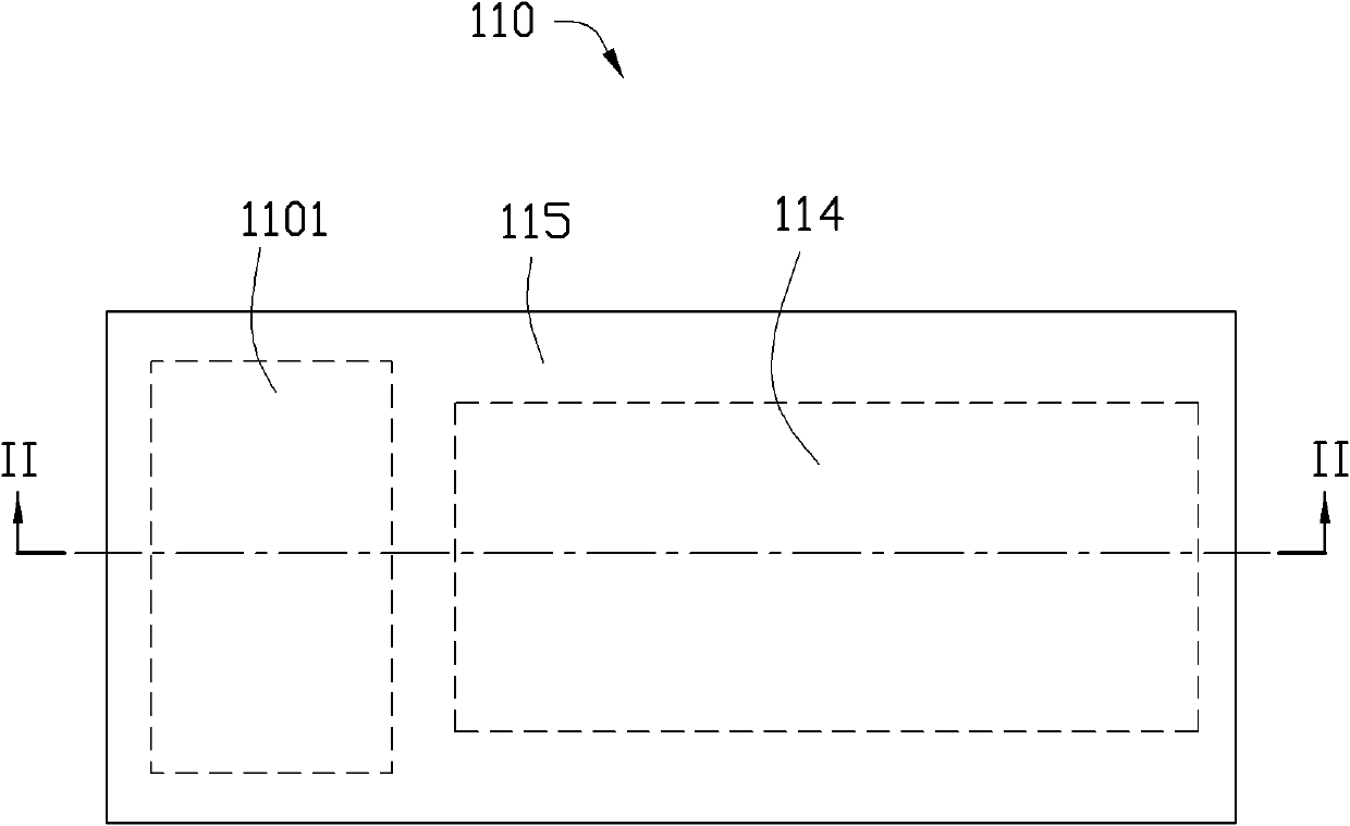
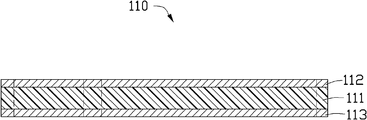
[0074] For the first step, please also refer to figure 1 with figure 2 , providing an inner layer substrate 110 .

[0075] The inner substrate 110 has a structure composed of conductive layers on both sides and an insulating layer between the two conductive layers. In this embodiment, the inner substrate 110 is a double-sided copper-clad substrate, which includes an insulating layer 111 and a first copper foil layer 112 and a fourth copper foil layer 113 formed on opposite sides of the insulating layer 111 . The inner substrate 110 includes a product area 114 and a non-product area 115 . The product area 114 corresponds to the circuit board unit to be formed, ...


PUM


Abstract

A manufacturing method of circuit boards includes steps of providing an inner substrate which comprises at least one product area and at least one test area arranged outside the product areas; manufacturing and forming a first conductive circuit in each product areas; forming first stopping laser graphics in the test areas; pressing first rubber layers and second copper foil layers; forming a second conductive circuit in each product area and forming first test graphics in the test areas; pressing second rubber layers and third copper foil layers, forming first product holes in the corresponding second copper foil layers and the second rubber layers in the product areas, forming a plurality of first test holes in the test areas, forming a first conductive layer in each first product hole, forming a second conductive layer in each first test hole, forming third conductive circuits and second test graphics in the second copper foil layers, and testing conductivity of the first test graphics and the second test graphics, thereby judging conduction conditions among the first conductive layers of the first product holes, the second conductive circuits and the third conductive circuits.

Description

technical field [0001] The invention relates to the technical field of circuit boards, in particular to a method for manufacturing a circuit board. Background technique [0002] Printed circuit boards have been widely used due to their advantages such as high assembly density. For the application of high-density interconnect circuit boards, please refer to the literature Takahashi, A.Ooki, N.Nagai, A.Akahoshi, H.Mukoh, A.Wajima, M.Res.Lab, High density multilayer printed circuit board for HITAC M- 880, IEEE Trans. on Components, Packaging, and Manufacturing Technology, 1992, 15(4): 418-425. [0003] In recent years, as the density of circuit boards continues to increase, the aperture of the interlayer via hole is also getting smaller and smaller. In this way, the reliability of the formed interlayer via hole cannot be guaranteed. Usually, the via holes in the circuit board are sampled and inspected after the circuit board is manufactured. The methods currently used are ge...

Claims


Application Information

Patent Timeline
Patent Type & Authority Patents(China)
IPC IPC(8): H05K3/40G01R31/28
Inventor 杨建朝唐莺娟
Owner HONGQISHENG PRECISION ELECTRONICS (QINHUANGDAO) CO LTD
Why Eureka
Try Eureka