Process monitoring method after metal gate cmp

A metal gate and metal technology, applied in the direction of instruments, semiconductor/solid-state device testing/measurement, measuring devices, etc., can solve problems such as slow measurement efficiency, complex device structure, process monitoring restrictions, etc., to avoid destructive testing, device Effect of Reliability Improvement

Active Publication Date: 2015-08-05
INST OF MICROELECTRONICS CHINESE ACAD OF SCI
View PDF6 Cites 0 Cited by
  • Summary
  • Abstract
  • Description
  • Claims
  • Application Information

AI Technical Summary

Problems solved by technology

With the continuous shrinking of technology nodes, device structures are becoming more and more complex, and stacked materials are getting thinner and thinner. Traditional optical measurement methods have encountered great challenges.
For process monitoring after the metal CMP process, traditional optical measurement systems cannot be used for measurement. The fundamental reason is that the light emitted by the light source cannot penetrate the metal material; for complex metal stack structures, optical measurement methods can only use indirect monitoring. The thickness of the insulating layer near the metal is used to monitor the CMP process, and this method requires a reflective layer under the measured insulating layer. Therefore, traditional optical measurement methods are greatly limited in the process monitoring after metal CMP.
At present, conventional metal CMP has tungsten (W) and copper (Cu) CMP processes; after the W CMP process, the thickness of the insulating layer is generally not monitored or indirectly monitored; after the Cu CMP process, the measurement using the principle of pulsed ultrasonic is more widely used. method, but the measurement efficiency of this method is much slower than optical measurement

Method used


Image

  • Process monitoring method after metal gate cmp
  • Process monitoring method after metal gate cmp
  • Process monitoring method after metal gate cmp

Examples


Embodiment Construction

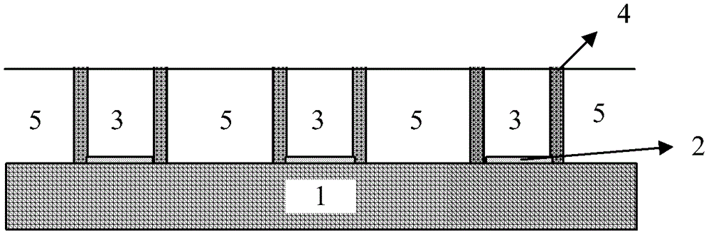
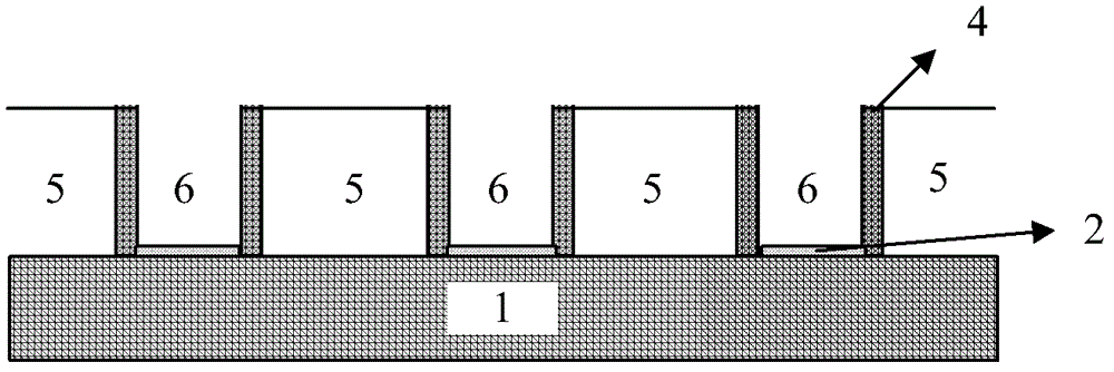
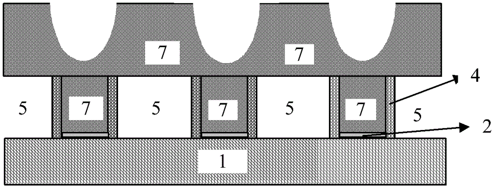
[0021] The features and technical effects of the technical solution of the present invention will be described in detail below with reference to the accompanying drawings and in conjunction with schematic embodiments. It is disclosed that the use of XRR measurement technology to monitor the metal gate CMP process of the last gate process is proposed, and the corresponding the test structure. It should be noted that similar reference numerals denote similar structures.

[0022] The metal gate CMP process that forms the gate structure is a new type of advanced CMP process with a technology node of 32nm and below. How to effectively monitor the metal gate CMP process has not been reported yet. The present invention proposes a measurement method based on X-ray reflectivity (XRR for short) to solve the above technical problems. The application of this technology in the integrated circuit industry is just in its infancy, and it is a process monitoring method with great development ...


PUM


Abstract

The invention provides a processing procedure monitoring method after CMP (Chemical Mechanical Polishing) for a metal gate. The processing procedure monitoring method comprises the steps as follows: a metal gate structure and a testing structure are formed on the surface of a wafer; a thickness measuring target of metal gate material and the error range are determined; metal in the metal gate structure and the testing structure is processed through CMP; and an XRR (X-ray Reflectivity) device is utilized to measure the thickness of the metal gate material in the testing structure, and whether the CMP technology is qualified is judged. According to the measuring method, the XRR device and the technology are adopted, and a destructive test on the wafer can be avoided, so that the testing and monitoring process can be more efficient, and the reliability of devices can be improved. In addition, the embodiment of the processing procedure monitoring method selects the measurement on the thickness of the metal gate, and the technical personnel in the field can also expand the monitoring method to the monitoring on the components of other semiconductor devices according to the spiritual essence of the processing procedure monitoring method.

Description

technical field [0001] The invention relates to a manufacturing method of a semiconductor device, in particular to a process monitoring method after metal gate chemical mechanical planarization. Background technique [0002] With the successful application of high-K / metal gate engineering on the 45nm technology node, it has become an indispensable key modular project for the sub-30nm technology node. At present, only Intel, which adheres to the high-K / gate last route, has achieved success in mass production at 45nm and 32nm. In recent years, Samsung, TSMC, Infineon and other industry giants following the IBM industry alliance have also shifted the focus of previous development from high-K / gate first to gate last engineering. [0003] For gate last engineering, the development of chemical mechanical planarization (CMP) process is considered the most challenging in the industry. In the gate last project, a CMP process is required to grind off the silicon oxide and silicon ni...

Claims


Application Information

Patent Timeline
Patent Type & Authority Patents(China)
IPC IPC(8): H01L21/66G01B15/02
Inventor 杨涛赵超李俊峰闫江陈大鹏
Owner INST OF MICROELECTRONICS CHINESE ACAD OF SCI
Why Eureka
Try Eureka