

Thin-film transistor
A technology of thin film transistors and oxide semiconductors, which is applied in the manufacture of transistors, semiconductor devices, semiconductor/solid-state devices, etc. It can solve the problems of TFT threshold voltage changes, current reduction, display size limitations, etc., and achieve the reduction of threshold voltage changes , The effect of reducing fluctuations in threshold voltage
Inactive Publication Date: 2012-07-04
CANON KK
View PDF6 Cites 14 Cited by
- Summary
- Abstract
- Description
- Claims
- Application Information
AI Technical Summary
Problems solved by technology
In addition, there are problems that driving the TFT for a long time causes a change in the threshold voltage of the TFT and a decrease in the current passing through the organic EL device.
[0005] Regarding low-temperature polysilicon TFTs, the circuit is complicated by the need to correct the circuit to overcome the inhomogeneity caused by the excimer laser used when crystallizing the silicon
In addition, there are problems such as that it is difficult to achieve a large display size because the display size is limited by the irradiation size of the excimer laser
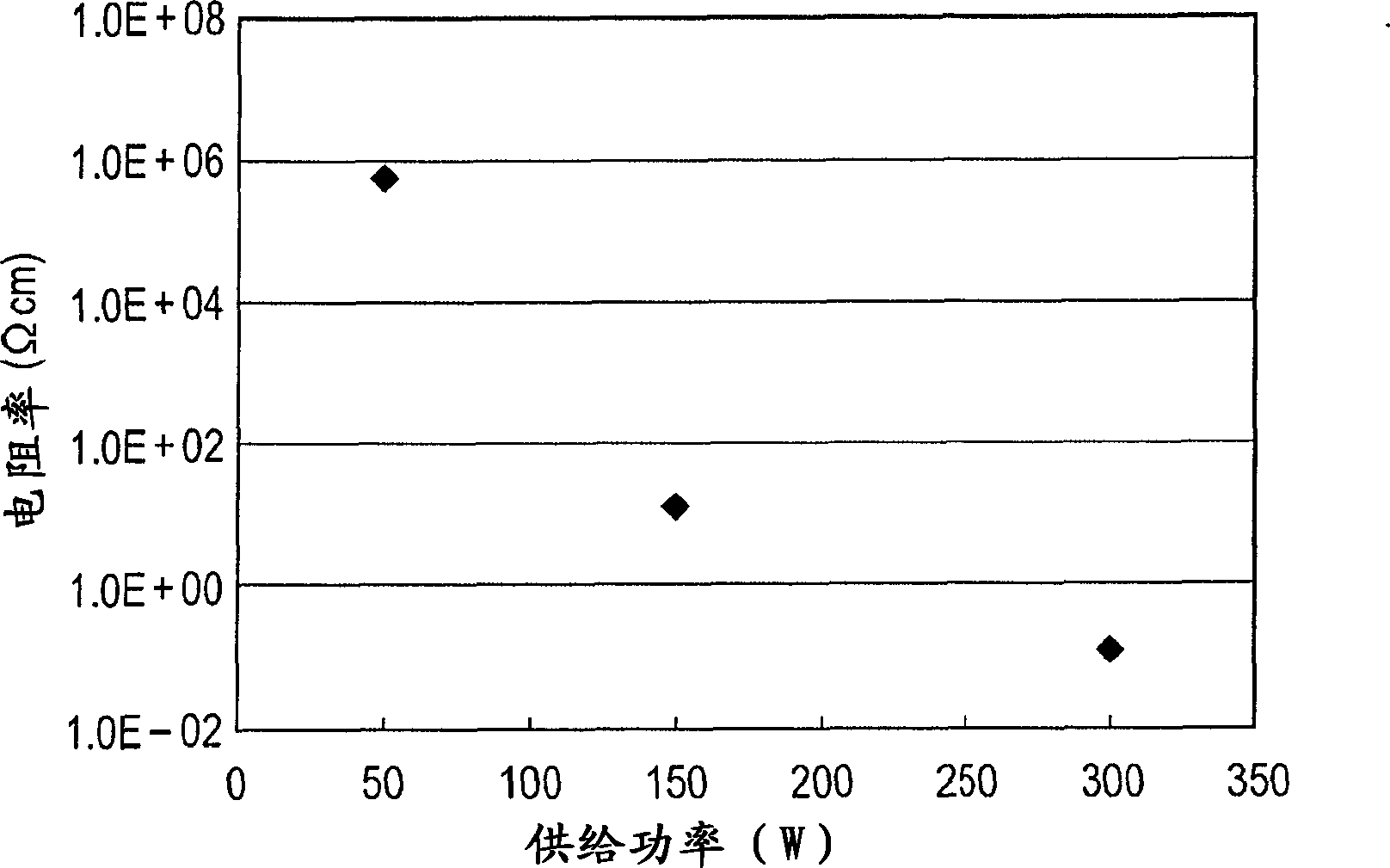
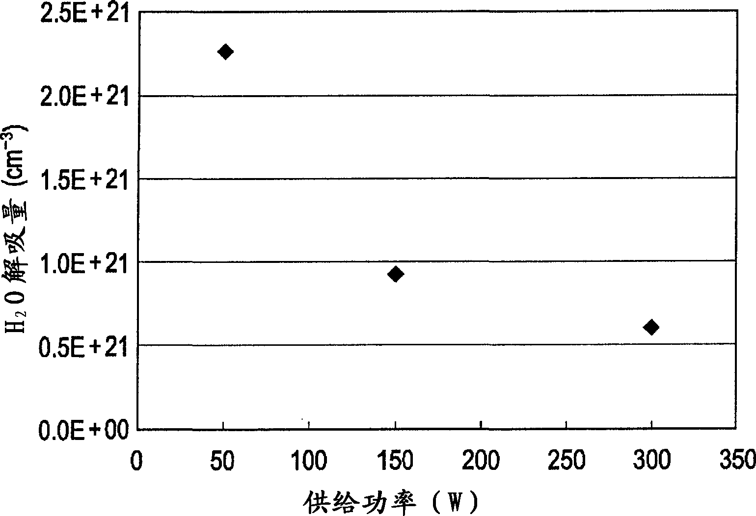
[0009] When such a protective layer is formed by a plasma chemical vapor deposition method (CVD method), a sputtering method, etc., for example, damage caused by plasma to a channel layer composed of an oxide semiconductor or hydrogen diffusion from the protective layer degrades the TFT. Deterioration of characteristics
Method used
View moreImage
Smart ImageViewing Examples

Examples
Embodiment Construction
[0039] Embodiments for carrying out the present invention will be described below with reference to the drawings.
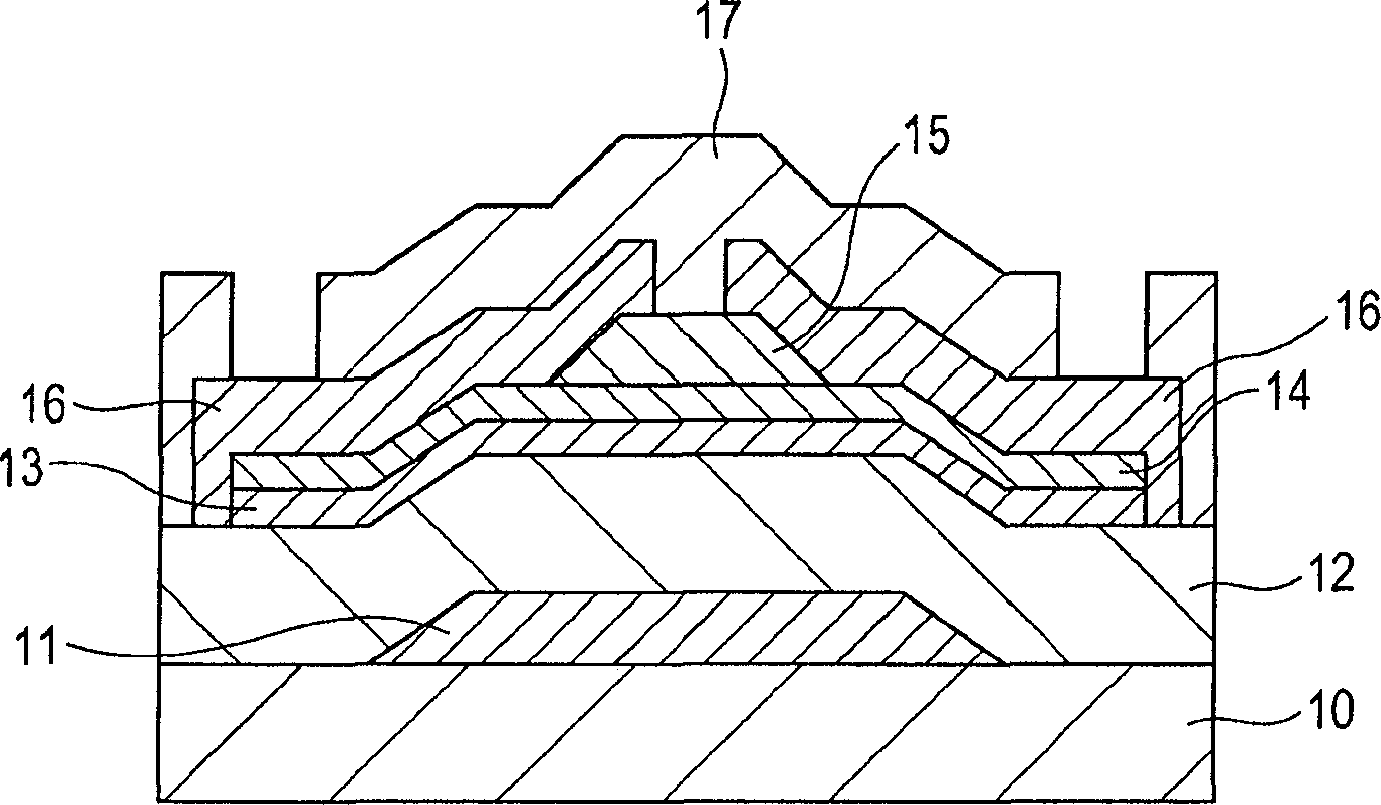
[0040] figure 1 It is a cross-sectional view showing the configuration of a bottom gate channel protection type oxide semiconductor TFT as a representative example of the present invention.
Login to View More PUM
 Abstract
Disclosed is an oxide semiconductor thin-layer transistor in which the threshold voltage for electric stress is stable and the variation in threshold voltage in transfer characteristics is minimized. Specifically disclosed is a thin-film transistor comprising an oxide semiconductor layer and a gate insulating layer provided in contact with the oxide semiconductor layer. The thin-film transistor is characterized in that the oxide semiconductor layer contains hydrogen atoms and has a region which functions as an active layer of the oxide semiconductor, the region has at least two regions having different average hydrogen concentrations along the thickness direction of the layer, that is, a first region and a second region in that order as viewed from the gate insulating layer side, and the average hydrogen concentration of the first region is lower than that of the second region.
Description
technical field [0001] The present invention relates to a thin film transistor including an oxide semiconductor and a method of manufacturing the thin film transistor. Background technique [0002] Currently, thin film transistors (TFTs) using amorphous silicon or low-temperature polysilicon for the semiconductor layer are being widely used as switching devices or driving devices in display devices such as active matrix type liquid crystal display devices or organic electroluminescent (EL) devices . [0003] However, since a high-temperature process is required to manufacture such a TFT, it is difficult to use a flexible substrate having low heat resistance such as a plastic substrate or a film substrate. [0004] When amorphous silicon TFTs are used as driving devices for organic EL devices, due to the low field effect mobility (up to 1cm 2 V -1 the s -1 ), so a TFT with a large size is required and it is difficult to reduce the size of a pixel. In addition, there are ...
Claims
Login to View More Application Information
Patent Timeline
 Patent Type & AuthorityApplications(China)
IPC IPC(8): H01L29/786H01L21/336
CPCH01L29/7869
Inventor佐藤步云见日出也林享渡边智大
OwnerCANON KK