Nickel alloy light guide plate cavity
A technology of nickel alloy and light guide plate, which is applied in the field of light guide plate, can solve the problems of time-consuming, diamond tool breakage, high cost, etc., and achieve the effect of good surface roughness and fast production cycle
- Summary
- Abstract
- Description
- Claims
- Application Information
AI Technical Summary
Problems solved by technology
Method used
Image
Examples
Example Embodiment
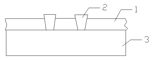
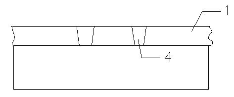
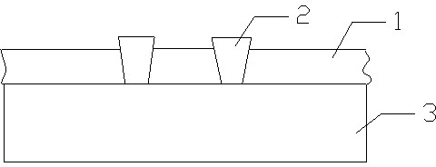
[0013] The figure shows a preferred embodiment of the present invention. The present invention will be further described with reference to the accompanying drawings. Among them, 1 electroformed nickel layer, 2 photoresist pattern, 3 substrate, 4 micropores.
[0014] figure 1 It is a schematic diagram of the structure of the nickel alloy light guide plate mold core of the present invention; the nickel alloy light guide plate mold core includes a substrate 3, a photoresist film (not shown completely) coated on the substrate 3, and electroforming deposited on the surface of the photoresist film and On the surrounding electroformed nickel layer 1, the photoresist film is provided with a photoresist film pattern (ie, photoresist pattern 2), and the electroformed nickel layer 1 is provided with a plurality of uniform micropores 4. The substrate 3 is used as a base, and the material is a silicon wafer; a mask plate (ie, a mask) with a certain three-dimensional pattern is produced accordi...
PUM
| Property | Measurement | Unit |
|---|---|---|
| Hardness | aaaaa | aaaaa |
Abstract
Description
Claims
Application Information


