Tool for mounting solder ball

A mounting and solder ball technology, which is applied in the direction of electrical components, semiconductor/solid-state device manufacturing, circuits, etc., can solve the problems of increasing the cost of BGA packaging process, and achieve the effect of cost saving

Active Publication Date: 2012-07-11
SAMSUNG SEMICON CHINA RES & DEV +1
View PDF5 Cites 1 Cited by
  • Summary
  • Abstract
  • Description
  • Claims
  • Application Information

AI Technical Summary

Problems solved by technology

However, in the existing BGA packaging process, since the through-hole layout of the solder ball placement tool is consistent with the pad layout of the package that needs to be solder ball mounted, it is difficult to perform solder ball bonding on packages with different pad layouts. When installing, it is necessary to make and replace different placement tools, which increases the cost of the BGA packaging process

Method used


Image

  • Tool for mounting solder ball
  • Tool for mounting solder ball
  • Tool for mounting solder ball

Examples


Embodiment Construction

[0028] The present invention is described more fully hereinafter with reference to the accompanying drawings, in which exemplary embodiments of the invention are shown. However, this invention may be embodied in many different forms and should not be construed as limited to the embodiments set forth herein. Rather, these embodiments are provided so that this disclosure will be thorough and complete, and will fully convey the scope of the invention to those skilled in the art. In the drawings, the size and relative sizes of layers and regions may be exaggerated for clarity.

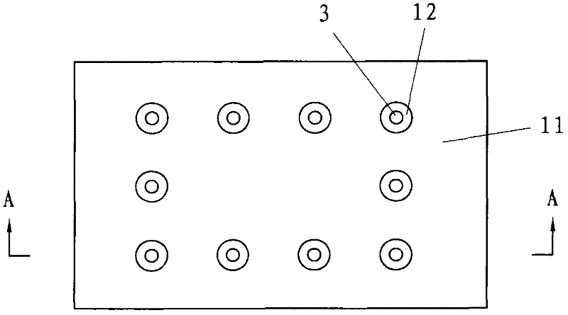
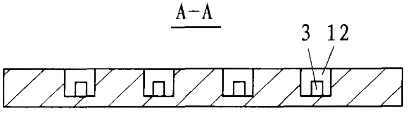
[0029] Figure 1a is a schematic top view showing a solder ball placement tool according to the prior art; Figure 1b is showing Figure 1a A schematic cross-sectional view taken along line A-A of a solder ball placement tool according to the prior art in .

[0030] refer to Figure 1a and Figure 1b , usually in order to achieve the purpose of mounting solder balls on the surface of the package, the pr...


PUM


Abstract

The invention discloses a tool for mounting a solder ball. The tool for mounting the solder ball comprises an upper solder ball mounting mould, a lower solder ball mounting mould, thimbles and a mask layer, wherein the upper solder ball mounting mould is internally provided with a plurality of through holes provided with predetermined patterns; the upper solder ball mounting mould is internally provided with a plurality of openings with predetermined patterns, and the openings formed in the lower solder ball mounting mould correspond to the through holes formed in the upper solder ball mounting mould one to one; the thimbles are arranged at the bottoms of the openings formed in the lower solder ball mounting mould; the mask layer is arranged between the upper solder ball mounting mould and the lower solder ball mounting mould and through holes with the predetermined patterns are formed in the mask layer.

Description

technical field [0001] The present invention relates to a solder ball placement tool, more specifically, the present invention relates to a solder ball that can be applied to a package structure with different solder ball numbers and solder ball layouts with the same package size and solder ball pitch Placement tools. Background technique [0002] With the development of integrated circuit technology, the packaging requirements for integrated circuits are more stringent. This is because the packaging technology is related to the functionality of the product. When the frequency of the IC exceeds 100MHz, the traditional packaging method may produce the so-called "CrossTalk (crosstalk)" phenomenon, and when the number of pins of the IC is greater than 208Pin, the traditional packaging method The method has its difficulties. Therefore, in addition to using the QFP packaging method, most of today's high-pin-count chips (such as graphics chips and chipsets, etc.) have turned to ...

Claims


Application Information

Patent Timeline
Patent Type & Authority Applications(China)
IPC IPC(8): H01L21/60
Inventor 黎英
Owner SAMSUNG SEMICON CHINA RES & DEV
Why Eureka
Try Eureka