Semiconductor apparatus and method for manufacturing the semiconductor apparatus

A semiconductor and plasma technology, which is applied in semiconductor/solid-state device manufacturing, semiconductor devices, electric solid-state devices, etc., can solve the problems of HEMTs that are difficult to obtain stable operating characteristics, and achieve the effect of reducing the etching rate

Active Publication Date: 2012-07-11
FUJITSU LTD
View PDF6 Cites 6 Cited by
  • Summary
  • Abstract
  • Description
  • Claims
  • Application Information

AI Technical Summary

Problems solved by technology

As a result, it becomes difficult for HEMTs to obtain stable operating characteristics

Method used


Image

  • Semiconductor apparatus and method for manufacturing the semiconductor apparatus
  • Semiconductor apparatus and method for manufacturing the semiconductor apparatus
  • Semiconductor apparatus and method for manufacturing the semiconductor apparatus

Examples


no. 1 example

[0027] (semiconductor device)

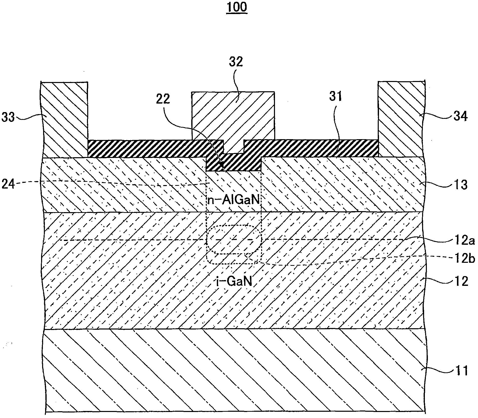
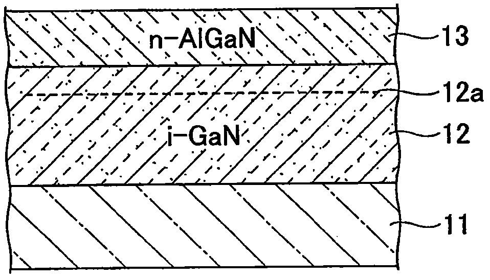
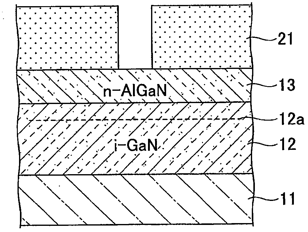
[0028] see figure 1 A semiconductor device 100 according to a first embodiment of the present invention is described. figure 1 It is a schematic diagram showing a semiconductor device 100 according to a first embodiment of the present invention. The semiconductor device 100 has semiconductor layers including an electron transport layer 12 and an electron supply layer 13 formed in this order on a substrate 11 . Substrate 11 is formed of a semi-insulating material such as SiC. The electron transport layer (to be the first semiconductor layer) 12 is formed of, for example, i-GaN. The electron supply layer (to be the second semiconductor layer) 13 is formed of, for example, n-AlGaN. Thus, a two-dimensional electron gas (2DEG) layer 12 a is formed in the electron transport layer 12 near the interface between the electron transport layer 12 and the electron supply layer 13 . Gate groove 22 is formed, for example, in electron supply layer 13 . Th...

no. 2 example

[0047] (semiconductor device)

[0048] see Figure 7 A semiconductor device 200 according to a second embodiment of the present invention is described. In the second embodiment, like elements are described using like reference numerals to those of the first embodiment without further description. Figure 7 It is a schematic diagram showing a semiconductor device 200 according to a second embodiment of the present invention. The semiconductor device 200 has a plurality of semiconductor layers including an electron transport layer 12 , an electron supply layer 13 , and a cap layer 14 sequentially formed on a substrate 11 . Substrate 11 is made of Si, for example. The electron transport layer (to be the first semiconductor layer) 12 is made of i-GaN, for example. The electron supply layer (to be the second semiconductor layer) 13 is made of, for example, n-AlGaN. Thus, a two-dimensional electron gas (2DEG) layer 12 a is formed in the electron transport layer 12 in the vicini...

no. 3 example

[0063] (semiconductor device)

[0064] see Figure 11 A semiconductor device 300 according to a third embodiment of the present invention is described. In the third embodiment, similar elements are described using similar reference numerals to those of the first and second embodiments without further description. Figure 11 It is a schematic diagram showing a semiconductor device 300 according to a third embodiment of the present invention. The semiconductor device 300 has a plurality of semiconductor layers including an electron transport layer 12 , an electron supply layer 13 , a protective layer 15 , a capping layer 16 , and a capping layer 14 which are sequentially formed on a substrate 11 . Substrate 11 is made of GaN, for example. The protective layer 15 is made of n-GaN. The cap layer 16 is made of i-AlN. The electron transport layer (to be the first semiconductor layer) 12 is made of i-GaN. The electron supply layer (to be the second semiconductor layer) 13 is ma...


PUM


Abstract

The invention provides a semiconductor apparatus and method for manufacturing the semiconductor apparatus. The semiconductor apparatus includes a first semiconductor layer formed on a substrate, a second semiconductor layer formed on the first semiconductor layer, a gate recess formed by removing at least a portion of the second semiconductor layer, an insulation film formed on the gate recess and the second semiconductor layer, a gate electrode formed on the gate recess via the insulation film, source and drain electrodes formed on one of the first and the second semiconductor layers, and a fluorine containing region formed in at least one of a part of the first semiconductor layer corresponding to a region in which the gate recess is formed and a part of the second semiconductor layer corresponding to the region in which the gate recess is formed. The normally closed characteristic is obtained according to the semiconductor apparatus, and the yield of the semiconductor apparatus is improved, and the stable operation is realized.

Description

technical field [0001] Embodiments discussed herein relate to a semiconductor device and a method of manufacturing the semiconductor device. Background technique [0002] Nitride semiconductors such as GaN, AlN, InN, or mixed crystals thereof have a wide band gap and are used in high-output electronic devices and short-wavelength light-emitting devices. Among high-output electronic devices, technologies for FETs (Field Effect Transistors, particularly, HEMTs (High Electron Mobility Transistors)) are being developed (for example, see Japanese Laid-Open Patent Publication No. 2002-359256). HEMTs using nitride semiconductors are used in high-output / high-efficiency amplifiers, high-power switching devices, and the like. [0003] HEMTs used in these devices need to have characteristics such as "normally off" and high insulation resistance. From a safety standpoint, the normally-off characteristic is important for HEMTs. Various methods for obtaining normally-off characteristic...

Claims


Application Information

Patent Timeline
Patent Type & Authority Applications(China)
IPC IPC(8): H01L29/778H01L21/335
CPCH01L29/7787H01L29/66462H01L29/4236H01L29/2003H01L2224/0603H01L2224/4903H01L2224/48247H01L2224/48472H01L21/28008H01L21/3065H01L21/308H01L29/7788
Inventor 多木俊裕远藤浩
Owner FUJITSU LTD
Why Eureka
Try Eureka