Sub-wavelength surface plasma laser
A surface plasmon and laser technology, which is applied to the structure of optical waveguide semiconductors and other directions, can solve the problems of inability to balance mode field confinement capability and transmission loss.
- Summary
- Abstract
- Description
- Claims
- Application Information
AI Technical Summary
Problems solved by technology
Method used
Image
Examples
example
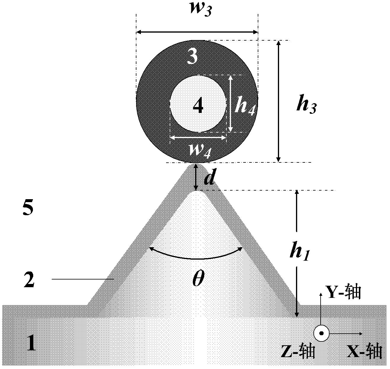
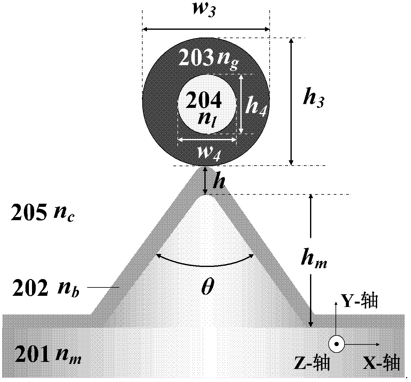
[0034] figure 2 is the cross-sectional structure diagram of the subwavelength surface plasmon laser described in the example. 201 is the metal base, n m Its refractive index, the inner vertex angle of the "∧"-shaped area is θ, and the height of the "∧"-shaped area is h m ; 202 is the medium buffer layer, n b is its refractive index, h is its thickness; 203 is a circular gain medium nanotube, n g is its refractive index, w 3 its width, h 3 Its height; 204 is the filling area in the center of the gain medium nanotube, n 1 is its refractive index, w 4 its width, h 4 Its height; 205 is the cladding, n c is its refractive index; the longitudinal (along the Z-axis direction) length of 201, 202, 203 and 204 is L.
[0035] In this example, the wavelength of the laser output light is 490nm, the material of 201 is silver, the real part of the refractive index at the wavelength of 490nm is -9.2, and the imaginary part is 0.3; the material of 203 is cadmium sulfide, and the real...
PUM
 Abstract
Description
Claims
Application Information


