Method for improving graphic precision of substractive process printed circuit board (PCB) by adopting dynamic etching compensation method

A subtraction method and compensation method technology, which is applied in the field of using the dynamic etching compensation method to improve the precision of the subtraction method PCB pattern, can solve the problems of the large difference in the size of the finished pattern, the difficulty of meeting the precision requirements of the isolated line and the line width, and the low precision ability. , to achieve the effect of effectively improving work efficiency, avoiding multiple modification of film, and improving production efficiency

Inactive Publication Date: 2012-07-11
DONGGUAN SHENGYI ELECTRONICS
View PDF4 Cites 47 Cited by
  • Summary
  • Abstract
  • Description
  • Claims
  • Application Information

AI Technical Summary

Problems solved by technology

When the DES (Developing / Etching / Stripping) production line is used to make the outer layer circuit, the greater the thickness of the bottom copper, the more difficult it is to control the line width accuracy, so the conventional etching compensation method is difficult to meet the high-speed development of PCB Dense line, isolated line line width precision requirements, different areas, different types of lines, and different types of graphics have large differences in the size of finished graphics, and the accuracy capability is relatively low, which cannot meet the terminal requirements

Method used


Image

  • Method for improving graphic precision of substractive process printed circuit board (PCB) by adopting dynamic etching compensation method
  • Method for improving graphic precision of substractive process printed circuit board (PCB) by adopting dynamic etching compensation method
  • Method for improving graphic precision of substractive process printed circuit board (PCB) by adopting dynamic etching compensation method

Examples


Embodiment Construction

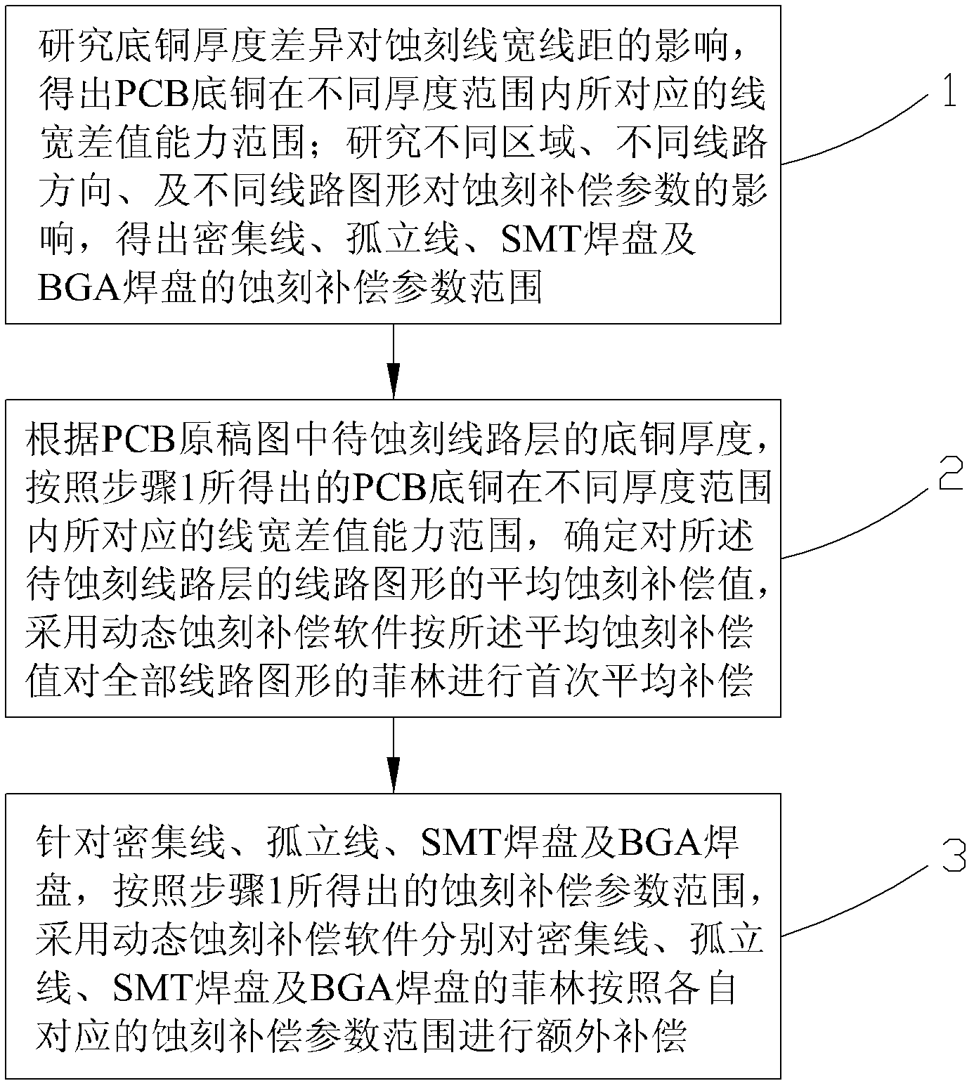
[0020] The present invention adopts the dynamic etching compensation method to improve the method for subtractive method PCB pattern precision, comprises the following steps:

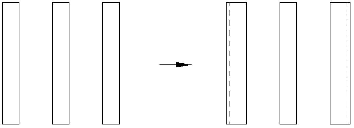
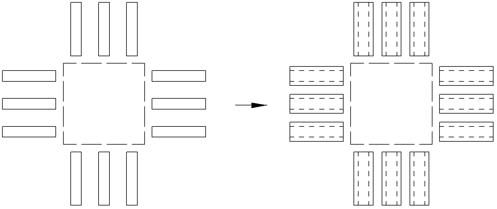
[0021] Step 1: Study the influence of bottom copper thickness difference on etching line width and line spacing, and obtain the corresponding line width difference capability range of PCB bottom copper in different thickness ranges; study different areas, different line directions, and different line patterns. Based on the influence of etching compensation parameters, the range of etching compensation parameters for dense lines, isolated lines, SMT pads and BGA pads is obtained.

[0022] The inventor designed a large number of experiments to study the line etching data of different bottom copper thicknesses. According to statistical data, the thicker the bottom copper, the greater the gap in line width, which is basically a positive correlation. When the bottom copper thickness differs by 10 μm, each lin...


PUM


Abstract

The invention relates to a method for improving the graphic accuracy of a substractive process printed circuit board (PCB) by adopting a dynamic etching compensation method. The method comprises the following steps of: step 1: studying the influence of thickness differences of base copper over etching line width and line distance so as to obtain the line width difference value ability ranges corresponding to the PCB base copper in different thickness ranges, and studying the influence of different areas, different line directions and different line graphs over etching compensation parameters so as to obtain etching compensation parameter ranges of compact lines, isolated lines, surface-mount technology (SMT) bonding pads and ball grid array (BGA) bonding pads; step 2: determining an average etching compensation value according to step 1 in accordance with the base copper thickness in an original draft of the PCB so as to firstly and averagely compensate films of all line graphs; and step 3: additionally compensating films of the compact lines, the isolated lines, the SMT bonding pads and the BGA bonding pads by adopting dynamic etching compensation software. By adopting the method disclosed by the invention, the influence of the base copper thickness, the etching uniformity and the like over the line width of the areas such as the compact lines, the isolated lines, the SMT bonding pads and the BGA bonding pads can be eliminated.

Description

technical field [0001] The invention relates to the field of circuit board production, in particular to a method for improving the accuracy of subtractive PCB graphics by adopting a dynamic etching compensation method. Background technique [0002] With the rapid development of electronic technology, for high-precision, high-density, high-frequency PCBs, customers require PCB finished copper bottom thickness, high graphics accuracy, small line width, and stricter requirements for outer layer impedance control and line width tolerance. Therefore, the equipment is required to have a stable and uniform line width output. When the DES (Developing / Etching / Stripping) production line is used to make the outer layer circuit, the greater the thickness of the bottom copper, the more difficult it is to control the line width accuracy, so the conventional etching compensation method is difficult to meet the high-speed development of PCB Dense line, isolated line width precision require...

Claims


Application Information

Patent Timeline
Patent Type & Authority Applications(China)
IPC IPC(8): H05K3/06
Inventor 杜红兵陶伟曾志军纪成光任尧儒
Owner DONGGUAN SHENGYI ELECTRONICS
Why Eureka
Try Eureka