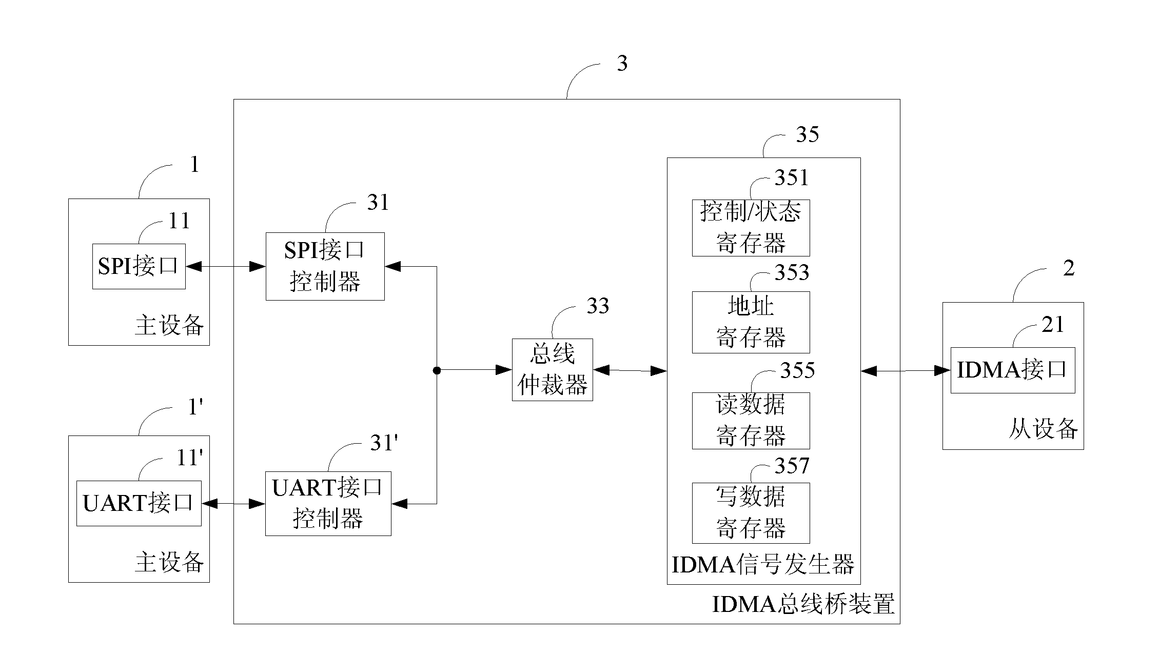
IDMA (interleave division multiple access) bus bridge device
A technology of IDMA and bus bridge, applied in the field of IDMA bus bridge device, can solve problems such as multi-operation time, cost, and undesired read operations, and achieve the effect of improving efficiency and safety
- Summary
- Abstract
- Description
- Claims
- Application Information
AI Technical Summary
Problems solved by technology
Method used
Image
Examples
example 1
[0069] Example 1: Address 0x1234 in master device 1 and slave device 2 ( Figure 4A Indicated by Addr_r) to read the data, as in Table 1 and image 3 Under the specification of the state transition relationship shown, the read operation can only be completed normally by performing the following steps:
[0070] Once the master device 1 executes step (1c)—write 0x1234 in the address register 353 of the IDMA signal generator 35 through the SPI interface controller 31, the IDMA signal generator 35 is based on the transition conditions shown in Table 1, Transition from idle state to address updated state. According to the action under the current state shown in table 1, IDMA signal generator 35 will produce the IDMA signal under the updated state of address (as Figure 4A As shown), the chip select signal is pulled low, and 0x1234 is put on the data input signal line, and then the address latch signal is pulled high, and the state position of the control / status register 351 is se...
example 6
[0107] Example 6: Insert the read operation of the IDMA signal generator 35 status checking step (2e). Master device 1 reads data from address 0x1234 in slave device 2, and slave device 2 responds.
[0108] Once the master device 1 executes step (1c)—write 0x1234 in the address register 353 of the IDMA signal generator 35 through the SPI interface controller 31, the IDMA signal generator 35 is based on the transition conditions shown in Table 1, Transition from idle state to address updated state. According to the action under the current state shown in table 1, IDMA signal generator 35 will produce the IDMA signal under the updated state of address (as Figure 4A As shown), the chip select signal is pulled low, and 0x1234 is put on the data input signal line, and then the address latch signal is pulled high, and the state position of the control / status register 351 is set to 0x1 at the same time.
[0109] Thus, the slave device 2 has received the signal of the address latch...
example 7
[0116] Example 7: Insert the read operation of the IDMA signal generator 35 status checking step (2e). Master device 1 reads data from address 0x1234 in slave device 2, and slave device 2 does not respond.
[0117] Once the master device 1 executes step (1c)—write 0x1234 in the address register 353 of the IDMA signal generator 35 through the SPI interface controller 31, the IDMA signal generator 35 is based on the transition conditions shown in Table 1, Transition from idle state to address updated state. According to the action under the current state shown in table 1, IDMA signal generator 35 will produce the IDMA signal under the updated state of address (as Figure 4A As shown), the chip select signal is pulled low, and 0x1234 is put on the data input signal line, and then the address latch signal is pulled high, and the state position of the control / status register 351 is set to 0x1 at the same time.
[0118] Thus, the slave device 2 has received the signal of the addre...
PUM
 Abstract
Description
Claims
Application Information


