Enhanced graphene field-effect transistor

A field-effect transistor, graphene technology, applied in the field of microelectronics and solid-state electronics, can solve the problems of no switching characteristics, no device saturation characteristics, etc.

Inactive Publication Date: 2012-07-18
SICHUAN UNIV
View PDF4 Cites 9 Cited by
  • Summary
  • Abstract
  • Description
  • Claims
  • Application Information

AI Technical Summary

Problems solved by technology

Now graphene is mainly used as the channel material of field effect transistors in transistors, but since graphene is a zero-bandgap semi-metal material and has a ballistic effect at room temperature, it is always in the "on" state when it is used as a device channel material. "state, there is no switching characteristic, and there is no device saturation characteristic

Method used


Image

  • Enhanced graphene field-effect transistor
  • Enhanced graphene field-effect transistor
  • Enhanced graphene field-effect transistor

Examples


Embodiment Construction

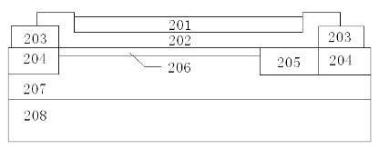
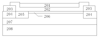
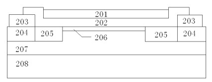
[0014] In order to overcome the field effect transistor using graphene as a channel, because it does not have the shortcomings of switching characteristics and saturation characteristics, the present invention proposes an enhanced graphene field effect transistor structure, by adopting the device structure of the present invention, Partially disconnect the graphene channel, such as disconnecting at the source, drain or source-drain at the same time, let the channel semiconductor doped layer replace the graphene layer, so that it can achieve switching characteristics and device saturation characteristics.

[0015] figure 1 , figure 2 with image 3 For the schematic diagram of the structure of the enhanced graphene field effect transistor implemented in the present invention, taking the N-type enhanced graphene field effect transistor as an example, the device structure includes: gate region 201, and the gate region material includes TiN, RuO2, Ru or other metals; the gate ...


PUM


Abstract

At present, graphene has become a hot research topic among domestic and foreign scientists. The graphene is now mainly used as a channel material of a field-effect transistor. However, the graphene is a zero gap material, has a ballistic effect at room temperature, and is always in an open state, so that the application of the graphene in the electronic field is limited. In order to overcome the shortcoming, the invention provides an enhanced graphene field-effect transistor, which belongs to the fields of microelectronics and solid state electronics. The enhanced graphene field-effect transistor comprises a gate region, a source region, a drain region, a channel region and a source and drain semiconductor doped region, wherein the channel region is formed by a graphene layer and a channel semiconductor doped layer; a N-type device channel semiconductor layer is doped with P-type impurities; and a P-type device channel semiconductor layer is doped with N-type impurities. By adoption of the device structure, the switching characteristic and saturation characteristic of the device can be realized, so that the graphene device can be well applied in an integrated circuit.

Description

technical field [0001] The invention belongs to the field of microelectronics and solid-state electronics, and relates to a semiconductor device, in particular to a novel enhanced graphene field effect transistor. Background technique [0002] At present, graphene has become a hot research topic for scientists at home and abroad, especially after two physicists from the University of Manchester won the Nobel Prize in Physics for their innovative research on graphene in 2010, it has aroused people's attention. extensive attention. At present, graphene is mainly used as the channel material of field effect transistors in transistors, but since graphene is a zero-bandgap semi-metal material and has a ballistic effect at room temperature, it is always in the "on" state when it is used as a device channel material. " state, there is no switching characteristic, and there is no device saturation characteristic. In view of the problems referred to above, the present invention pro...

Claims


Application Information

Patent Timeline
Patent Type & Authority Applications(China)
IPC IPC(8): H01L29/10H01L29/78
Inventor 石瑞英刘杰杜惊雷
Owner SICHUAN UNIV
Why Eureka
Try Eureka