Field-effect transistor fabrication method and field-effect transistor

A field effect transistor, two-dimensional semiconductor technology, applied in transistors, semiconductor/solid-state device manufacturing, semiconductor devices, etc., can solve the problems of too small output resistance, large source-drain voltage, stagnation of low-dimensional semiconductor applications, etc. The effect of operating voltage and power consumption, low cost, and simple structure

Inactive Publication Date: 2019-07-26
INST OF MICROELECTRONICS CHINESE ACAD OF SCI
View PDF5 Cites 2 Cited by
  • Summary
  • Abstract
  • Description
  • Claims
  • Application Information

AI Technical Summary

Problems solved by technology

However, there are still some key problems in this field that have not been resolved, such as: the source-drain voltage required for the transistor to reach saturation is too large, and the output resistance of the transistor is too small even when it reaches saturation, which leads to low-dimensional semiconductors in The application of analog circuits is still at a standstill

Method used


Image

  • Field-effect transistor fabrication method and field-effect transistor
  • Field-effect transistor fabrication method and field-effect transistor
  • Field-effect transistor fabrication method and field-effect transistor

Examples


Embodiment Construction

[0040] In order to make the object, technical solution and advantages of the present invention clearer, the present invention will be further described in detail below in conjunction with specific embodiments and with reference to the accompanying drawings.

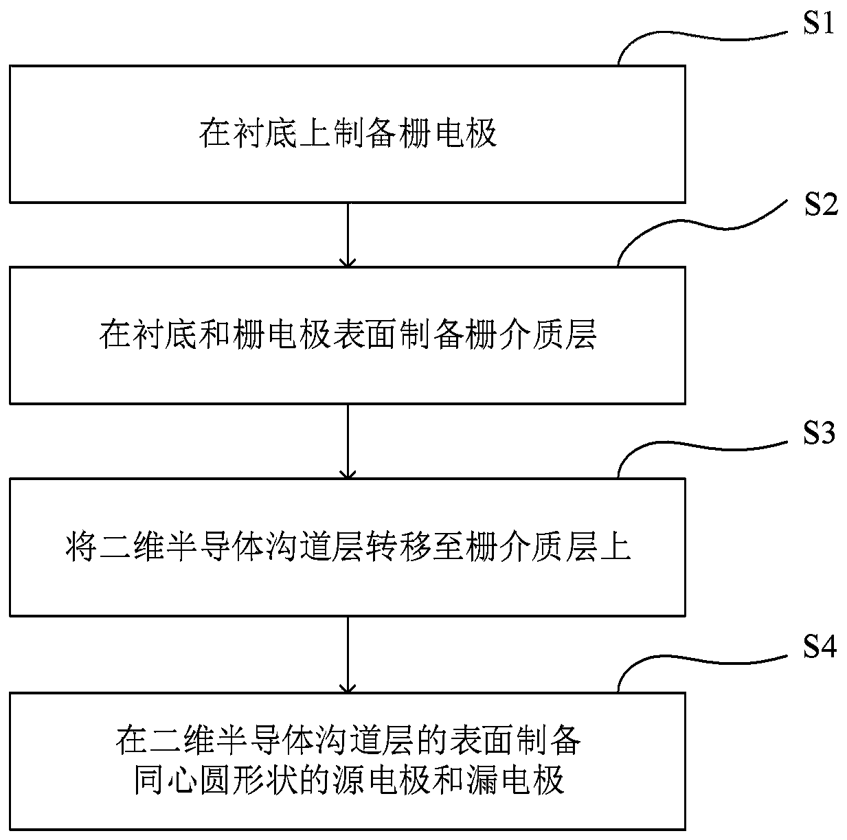
[0041] According to one aspect of the present invention, a kind of field effect transistor preparation method is provided, such as figure 1 As shown, the method includes the following steps:

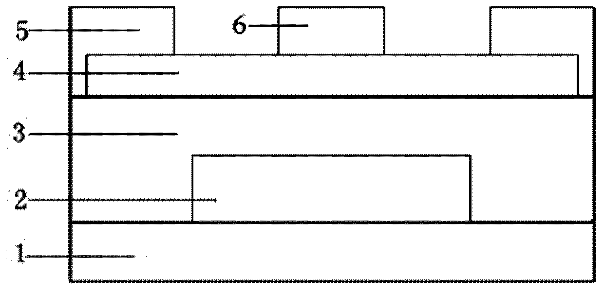
[0042] Step S1, preparing a gate electrode on the substrate;

[0043] Step S2, preparing a gate dielectric layer on the surface of the substrate and the gate electrode;

[0044] Step S3, transferring the two-dimensional semiconductor channel layer onto the gate dielectric layer;

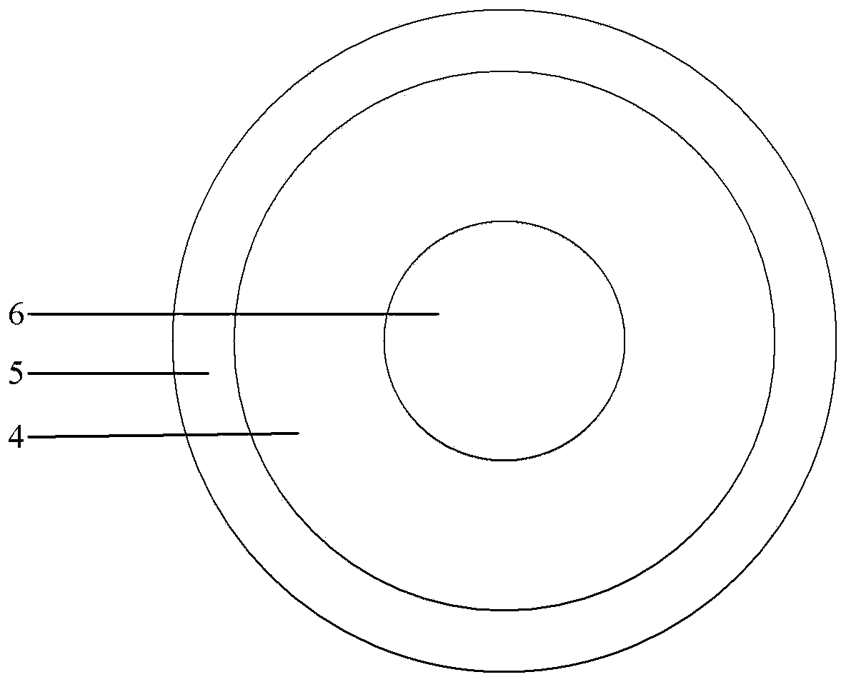
[0045] Step S4, preparing concentric circle-shaped source electrodes and drain electrodes on the surface of the two-dimensional semiconductor channel layer; wherein, the outer circle is the drain electrode, and the inner circle is the source electrode. ...


PUM


Abstract

The invention provides a field-effect transistor fabrication method and a field-effect transistor, and belongs to the technical field of field-effect transistor manufacturing. The field-effect transistor fabrication method comprises the steps of fabricating a gate electrode on a substrate; fabricating a gate dielectric layer on surfaces of the substrate and the gate electrode; transferring a two-dimensional semiconductor channel layer to the gate dielectric layer; and fabricating a source electrode and a drain electrode which are in a concentric shape on a surface of the two-dimensional semiconductor channel layer, wherein an outer circle is the drain electrode, and an inner circle is the source electrode. By different shapes of the source electrode and the drain electrode in the concentric shape, a high-field region is more easily generated between the source electrode and the drain electrode, so that saturation characteristic of the transistor under a relatively low source-drain voltage is achieved, and the operation voltage and the power consumption during the working process of the transistor are reduced.

Description

technical field [0001] The invention relates to the technical field of field effect transistor manufacturing, in particular to a method for preparing a field effect transistor and the field effect transistor. Background technique [0002] In the post-Moore era, traditional silicon-based three-dimensional field effect transistors are on the path of size reduction. Due to physical limitations such as short channel effects and increasingly high R&D and manufacturing costs, people have begun to pay attention to the application of two-dimensional semiconductors in this field. MoS 2 , MoSe 2 And other two-dimensional materials, because there are no dangling bonds, and there is no short channel effect in the case of a single layer or few layers, the cost is low and other reasons have become the focus of research. However, there are still some key problems in this field that have not been resolved, such as: the source-drain voltage required for the transistor to reach saturation i...

Claims


Application Information

Patent Timeline
Patent Type & Authority Applications(China)
IPC IPC(8): H01L29/786H01L29/417H01L21/34
CPCH01L29/41733H01L29/66969H01L29/786H01L29/78681
Inventor 卢年端揣喜臣杨冠华李泠耿玓刘明
Owner INST OF MICROELECTRONICS CHINESE ACAD OF SCI
Why Eureka
Try Eureka