Light emitting diode (LED) package method and structure

A technology of LED packaging and thermally conductive substrates, applied in lighting devices, lighting and heating equipment, electrical components, etc., can solve the problems of high control requirements for second welding parameters, low product yield, and increase production costs, and achieve flexible and convenient adjustment. The effect of light color tone, low LED junction temperature, and overall cost reduction

Active Publication Date: 2012-07-25
ZHEJIANG TAI G PHOTOELECTRIC TECH CO LTD
View PDF3 Cites 2 Cited by
  • Summary
  • Abstract
  • Description
  • Claims
  • Application Information

AI Technical Summary

Problems solved by technology

However, the existing LED packaging method has low production efficiency, low product yield, and chip bonding method is not conducive to the stability of the chip.
Most of the existing COB products are in the form of planar packaging, and the substrate structure does not reflect light well. Some light is reflected and absorbed by the internal reflection of the package, resulting in low light output efficiency.
Luminous efficiency can only reach 80% of LED in dual in-line package form
However, MCOB products have a greater impact on production capacity and cost due to the higher substrate structure and processing precision.
In addition, the existing LED substrate modules can only achieve series-parallel connection and welding between chips, and the control requirements for the second welding parameters are relatively high during the chip welding process
As a result, when one of the chips fails, it cannot be repaired alone and the entire substrate light source is scrapped
It greatly affects the production yield and increases the production cost

Method used


Image

  • Light emitting diode (LED) package method and structure
  • Light emitting diode (LED) package method and structure
  • Light emitting diode (LED) package method and structure

Examples


Embodiment Construction

[0017] The present invention will be further described below in conjunction with the accompanying drawings and embodiments, but not as a basis for limiting the present invention.

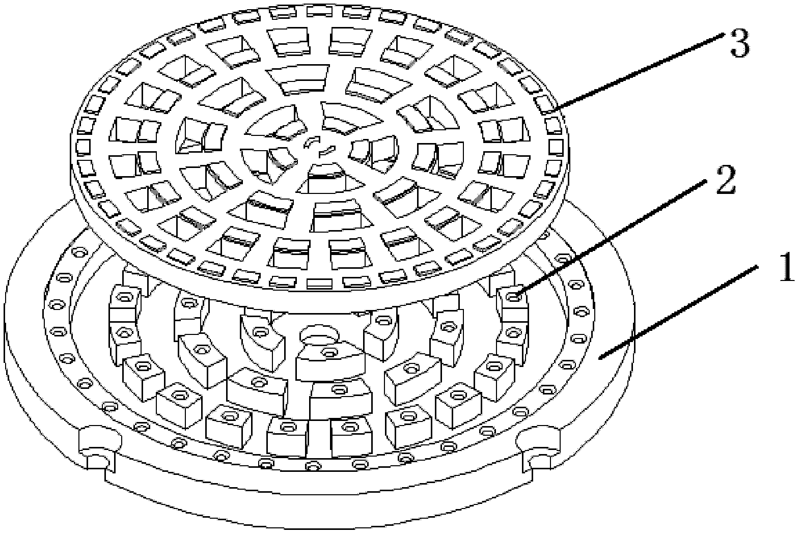
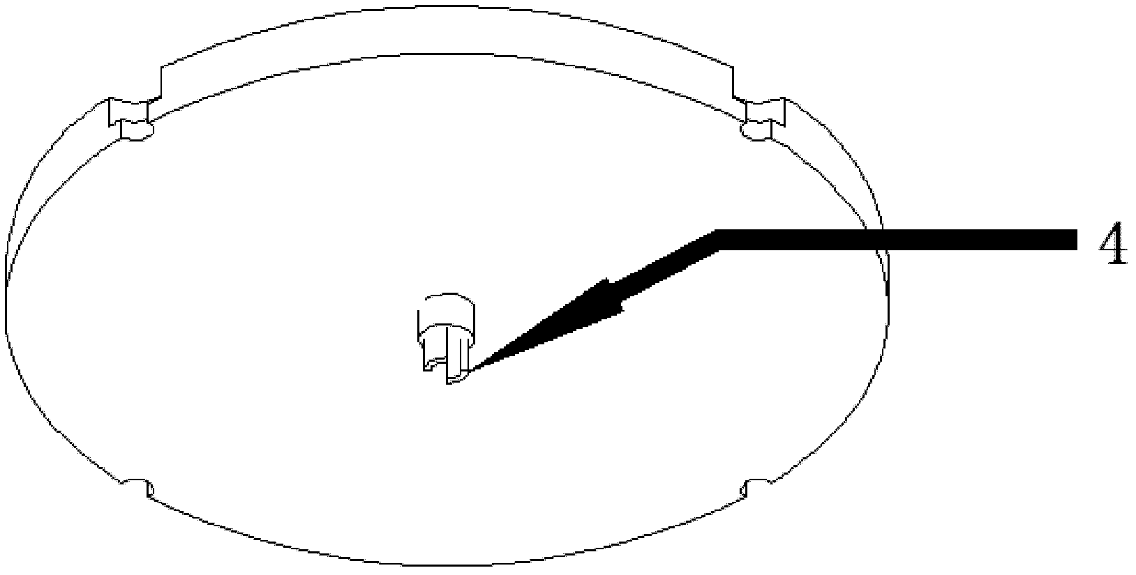
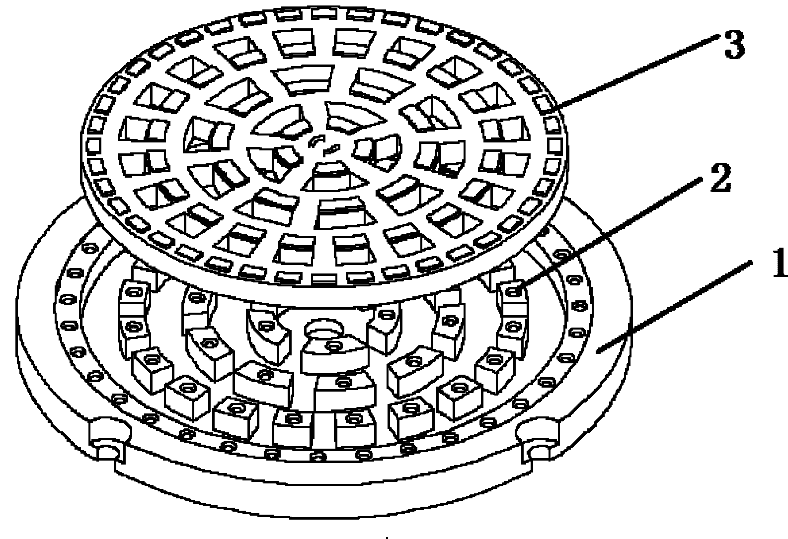
[0018] Example. The invention relates to an LED packaging method. A plurality of independent reflective grooves are set up on an integral heat-conducting substrate, LED chips are fixed in the reflective grooves, and fluorescent powder is injected into them to be baked and solidified. An integral wiring frame is embedded on the heat-conducting substrate, and the connection between each LED chip is realized by performing integral wiring on the wiring frame. The fluorescent powder is solidified into a cup shape. An extraction electrode is provided at the bottom of the heat-conducting substrate.

[0019] A kind of LED encapsulation structure that realizes above-mentioned method, such as figure 1 As shown, it includes a heat-conducting substrate 1, on which a reflective groove 2 is opened, and a high-...


PUM


Abstract

The invention discloses a light emitting diode (LED) package method and an LED package structure. A plurality of independent reflection slots are formed on an integrated heat conduction substrate; LED chips are fixedly arranged in the reflection slots; and fluorescent powder is injected into the reflection slots and used for solidifying the LED chips. According to the method and the structure, the stability and the light output efficiency of LEDs are improved; and furthermore, the requirement on LED package processing cost and precision can be reduced, and the yield and the production efficiency of an LED product are improved.

Description

technical field [0001] The invention relates to an LED packaging method and structure, belonging to the technical field of LED lighting. Background technique [0002] LED light-emitting diode lighting has the advantages of high efficiency and energy saving. The luminous efficiency of most current LED lighting lamps can exceed 70LM / W, which is more energy-saving than traditional energy-saving lamps. However, the existing LED packaging method has low production efficiency, low product yield rate, and chip bonding method is not conducive to the stability of the chip. Most of the existing COB products are in the form of planar packaging, and the substrate structure does not reflect light well. Some light is reflected and absorbed by the internal reflection of the package, resulting in low light output efficiency. The light efficiency can only reach 80% of that of the LED in the dual in-line package form. However, MCOB products have a greater impact on production capacity and c...

Claims


Application Information

Patent Timeline
Patent Type & Authority Applications(China)
IPC IPC(8): H01L33/00H01L33/64H01L33/60F21S2/00F21Y101/02F21K9/20F21Y115/10
Inventor 沈航
Owner ZHEJIANG TAI G PHOTOELECTRIC TECH CO LTD
Why Eureka
Try Eureka