
Solid-state storage system with parallel access of multiple flash/PCM devices

A technology for solid-state storage and storage systems, applied in static storage, instruments, error detection/correction, etc., and can solve problems such as increasing the complexity of storage systems

Active Publication Date: 2012-08-08
IBM CORP
View PDF4 Cites 2 Cited by
  • Summary
  • Abstract
  • Description
  • Claims
  • Application Information

AI Technical Summary

Problems solved by technology

However, this increases the complexity of the storage system implementation

Method used


Image

  • Solid-state storage system with parallel access of multiple flash/PCM devices
  • Solid-state storage system with parallel access of multiple flash/PCM devices
  • Solid-state storage system with parallel access of multiple flash/PCM devices

Examples


Embodiment Construction

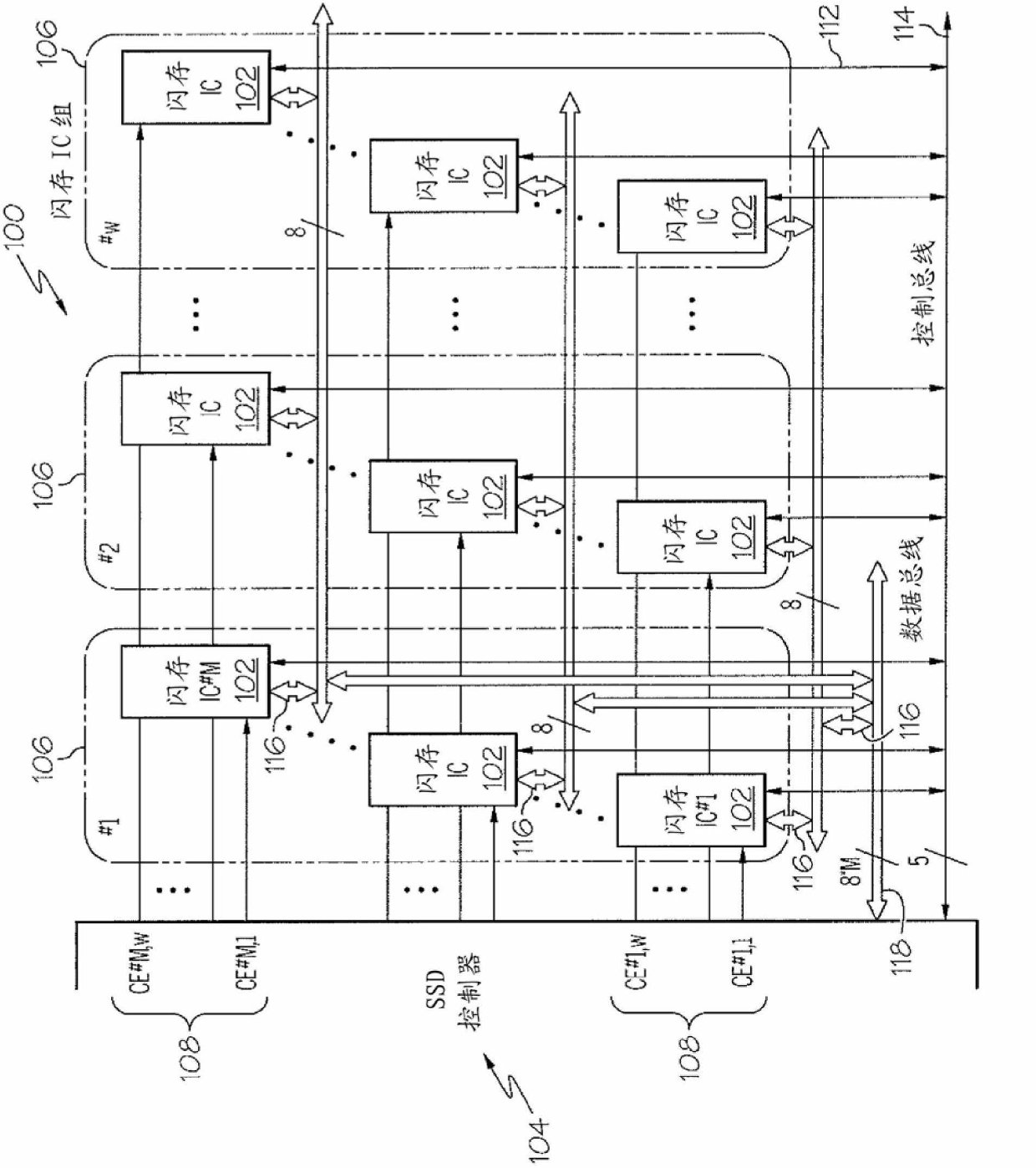
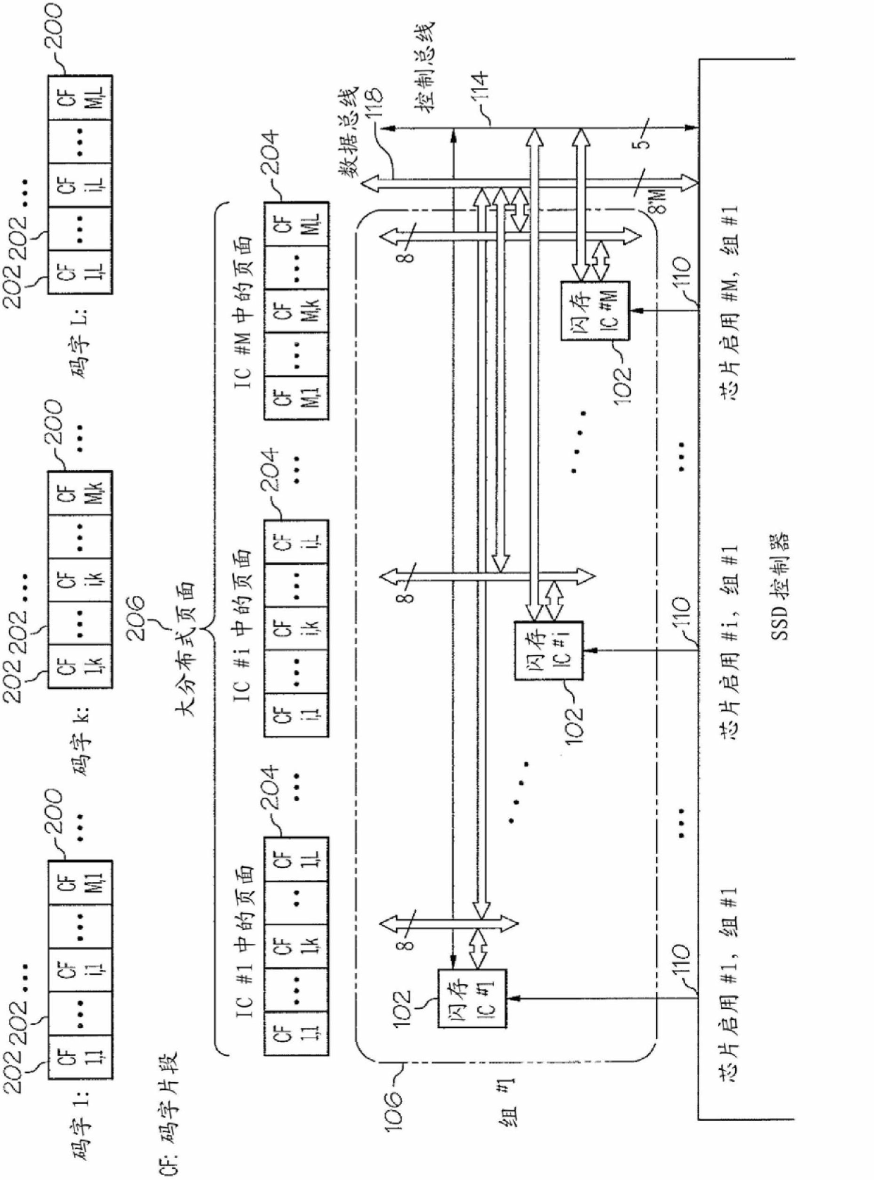
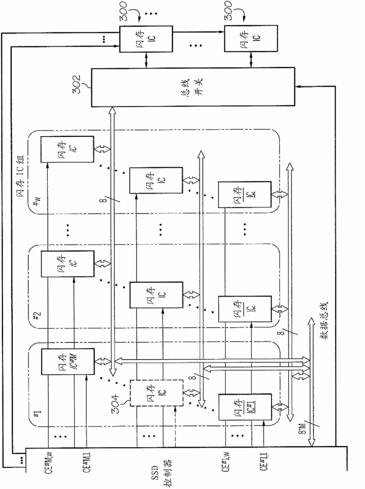
[0016] Exemplary embodiments of the present invention provide flash memory storage systems and methods that handle failures in solid-state drives (SSDs) by using a fault-tolerant architecture with error-correcting code (ECC) mechanisms and interleaving mechanisms for random / burst error correction Problems with memory integrated circuits (ICs). In general, the systems and systems described herein allow recovery of previously stored data from a failed integrated circuit and correction of random / burst errors in other functioning integrated circuits when one or more integrated circuits fail. method to keep the SSD running. These systems and methods replace a failed integrated circuit with a functional / fully functioning integrated circuit that is hereby considered as a spare integrated circuit. Additionally, the fault-tolerant architecture implemented in the exemplary embodiments can improve I / O performance in terms of achievable maximum read / write data rates.

[0017] The integr...


PUM


Abstract

Systems and methods are provided that confront the problem of failed storage integrated circuits (ICs) in a solid state drive (SSD) by using a fault-tolerant architecture along with one error correction code (ECC) mechanism for random / burst error corrections and an L-fold interleaving mechanism. The systems and methods described herein keep the SSD operational when one or more integrated circuits fail and allow the recovery of previously stored data from failed integrated circuits and allow random / burst errors to be corrected in other operational integrated circuits. These systems and methods replace the failed integrated circuits with fully functional / operational integrated circuits treated herein as spare integrated circuits. Furthermore, these systems and methods improve I / O performance in terms of maximum achievable read / write data rate.

Description

Background technique [0001] Currently, flash-based storage is the most common non-volatile RAM technology in solid-stat drives (SSDs), but it is foreseeable that in the near future, phase-change storage-class memory (phase-change storage-class memory, PCM) other technologies will be used in solid-state storage systems. A common way to achieve high-performance I / O is to use multiple independent channels that are accessed in parallel. The data rate achieved in each channel is primarily limited by the "Page Write" and "Page Read" times required internally by the flash device to complete the respective operations, and the clock rate at the device interface . [0002] Currently in SSDs, besides cost and I / O performance, one of the major issues with using flash chips or flash integrated circuit devices (ICs) is reliability and endurance issues due to the amount of write / erase that can be performed in the flash cells due to the limited number of division operations. This phenomen...

Claims


Application Information

Patent Timeline
IPC IPC(8): G06F11/10G11C29/00
CPCG11C29/765G06F11/1028
Inventor T.A.安托纳科波罗斯R.D.西德西扬E.S.艾勒夫瑟里奥R.哈斯胡晓宇I.伊利亚迪斯
Owner IBM CORP
Learn More