

Solid-state storage system with parallel access of multiple flash/PCM devices
A technology for solid-state storage and storage systems, applied in static storage, instruments, error detection/correction, etc., and can solve problems such as increasing the complexity of storage systems
- Summary
- Abstract
- Description
- Claims
- Application Information
AI Technical Summary
Problems solved by technology
Method used
Image

Examples
Embodiment Construction
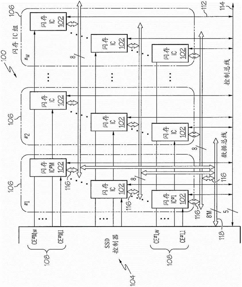
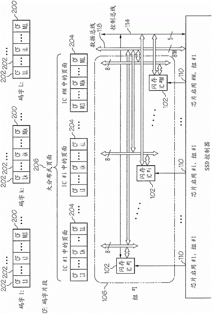
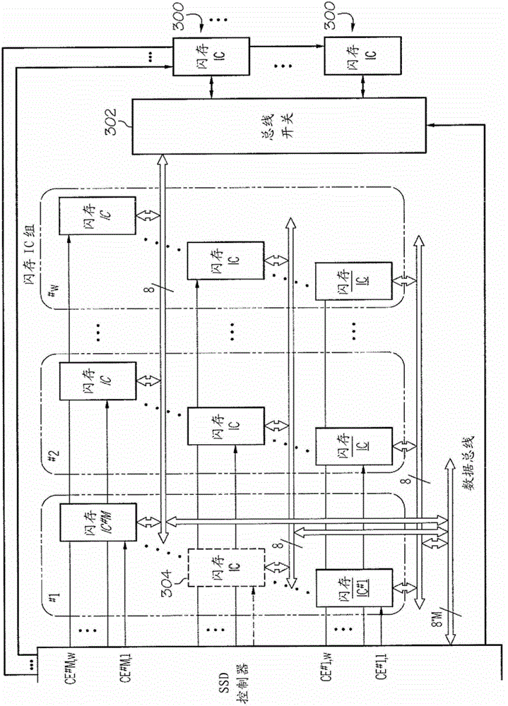
[0016] Exemplary embodiments of the present invention provide flash memory storage systems and methods that handle failures in solid-state drives (SSDs) by using a fault-tolerant architecture with error-correcting code (ECC) mechanisms and interleaving mechanisms for random / burst error correction Problems with memory integrated circuits (ICs). In general, the systems and systems described herein allow recovery of previously stored data from a failed integrated circuit and correction of random / burst errors in other functioning integrated circuits when one or more integrated circuits fail. method to keep the SSD running. These systems and methods replace a failed integrated circuit with a functional / fully functioning integrated circuit that is hereby considered as a spare integrated circuit. Additionally, the fault-tolerant architecture implemented in the exemplary embodiments can improve I / O performance in terms of achievable maximum read / write data rates.
[0017] The integr...
PUM
 Abstract
Description
Claims
Application Information