
Method for preventing phosphosilicate glass or boron phosphosilicate glass film from absorbing water

A technology of phosphosilicate glass and silicate glass, applied in electrical components, semiconductor/solid-state device manufacturing, circuits, etc., can solve the problems of increasing process cost, reducing product yield, controlling wafer waste, etc., and achieving savings Process cost, increased yield, simple and easy-to-operate process

Active Publication Date: 2015-03-11
SHANGHAI HUALI MICROELECTRONICS CORP
View PDF4 Cites 0 Cited by
  • Summary
  • Abstract
  • Description
  • Claims
  • Application Information

AI Technical Summary

Problems solved by technology

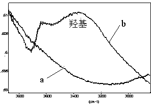
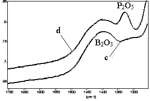
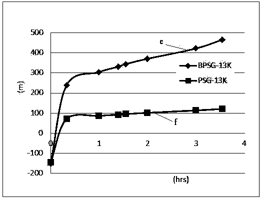
[0009] Figure 4 It is the current BPSG / PSG process flow diagram in the background technology of the present invention; as Figure 4 As shown, the current control methods are mainly adopted: ① For the product (Product wafer), the time from BPSG / PSG film deposition (dep) to anneal (Anneal) is 6 to 10 hours (Q time), if it exceeds this time period There is no way to re-work, only the anneal process (anneal) as soon as possible, and then the next process as soon as possible, which will result in a decrease in product yield
②For monitor wafers, because the film is unstable, after deposition, it is necessary to measure the corresponding parameters (such as thickness, concentration, stress, etc.) within three hours. The film cannot be used to evaluate the performance of the machine, but can only be re-deposited, which will cause waste of the control film and increase the process cost

Method used


Image

  • Method for preventing phosphosilicate glass or boron phosphosilicate glass film from absorbing water
  • Method for preventing phosphosilicate glass or boron phosphosilicate glass film from absorbing water
  • Method for preventing phosphosilicate glass or boron phosphosilicate glass film from absorbing water

Examples


Embodiment Construction

[0029] The specific embodiment of the present invention will be further described below in conjunction with accompanying drawing:

[0030] Figure 4 It is the current BPSG / PSG process flow chart in the background technology of the present invention;

[0031] Figure 5 It is a process flow diagram of the method for preventing phosphosilicate glass or borophosphosilicate glass film from absorbing water in the present invention;

[0032] Figure 6-8 It is a structural flow diagram of the method for preventing phosphosilicate glass or borophosphosilicate glass film from absorbing water in the present invention.

[0033] Such as Figure 4-8 As shown, first, deposit phosphosilicate glass or borophosphosilicate glass (BPSG / PSG) film 2 on a silicon substrate (Sisub) 1; then, at a temperature of 300-500°C, use plasma Enhanced Chemical Vapor Deposition (Plasma Enhanced Chemical Vapor Deposition, referred to as PECVD) process, depositing an amorphous carbon (amorphous carbon) film 3 w...


PUM

PropertyMeasurementUnit
thicknessaaaaaaaaaa

Abstract

The invention relates to the field of manufacture of semiconductors, in particular to a method for preventing phosphosilicate glass or boron phosphosilicate glass film from absorbing water. The method includes: depositing an amorphous carbon film layer on the phosphosilicate glass or boron phosphosilicate glass film, accordingly isolating reaction between the phosphosilicate glass or boron phosphosilicate glass film and external water vapor and the like and preventing the phosphosilicate glass or boron phosphosilicate glass film from being humidified by absorbing water so that the manufactured phosphosilicate glass or boron phosphosilicate glass film can be stored for a long time. Besides, the amorphous carbon film layer can be removed by common plasma ashing and cleaning with wet method when wafers with the phosphosilicate glass or boron phosphosilicate glass film are delivered, so that possibility of abandonment of the wafers can be reduced, yield of products can be increased, process cost is saved and process is simple and easy to operate.

Description

technical field [0001] The invention relates to the manufacturing field of semiconductor integrated circuits, in particular to a method for preventing water absorption of phosphosilicate glass or borophosphosilicate glass film. Background technique [0002] Phospho-silicate-glass (PSG) is a kind of SiO doped with phosphorus (P). 2 Glass. The incorporated P is mainly to capture mobile metal cations (mainly Na + ) and reduce the reflow temperature. Generally, the more P is added, the better the reflux effect will be. [0003] However, because the reflow temperature required by PSG is very high (generally around 1000°C), high temperature treatment is likely to cause re-diffusion of impurity concentration and deformation of the silicon wafer, and the content of P will affect the stability and reliability of the film. The more P is added, the easier it is to absorb water. Therefore, boro-phospho-silicate-glass (BPSG) doped with boron (B) appeared instead of PSG. amount to r...

Claims


Application Information

Patent Timeline
Patent Type & Authority Patents(China)
IPC IPC(8): H01L21/02
CPCY02P80/30
Inventor 肖海波郑春生胡学清
Owner SHANGHAI HUALI MICROELECTRONICS CORP
Learn More