Manufacturing process of interlayer copper connector of printed circuit board

A technology for printed circuit boards and manufacturing processes, which is applied in the direction of electrical connection formation of printed components to achieve the effects of reducing the total investment, reducing investment risks, and shortening the production cycle.

Inactive Publication Date: 2012-08-15
SHENZHEN HONGHAI ELECTRON MATERIAL TECH CO LTD
View PDF2 Cites 7 Cited by
  • Summary
  • Abstract
  • Description
  • Claims
  • Application Information

AI Technical Summary

Benefits of technology

This technology uses an easy-to operate method called screensprinting that combines two materials: one being made from liquid or solid material like epoxies while another containing electrically charged particles suspended therein. These techniques help create better electronic components on flexible substrates by improving their overall functionality without requiring expensive metallization processes such as electroplated nickel layers.

Problems solved by technology

This patented technical solution described in this patents involves improving printing circuitboards' ability to connect different parts together without requiring excessive manual effort or material costs associated therewith. By implementing these techniques, the cost savings result in improved efficiency and quality control over printed circuitry designs.

Method used


Image

  • Manufacturing process of interlayer copper connector of printed circuit board
  • Manufacturing process of interlayer copper connector of printed circuit board
  • Manufacturing process of interlayer copper connector of printed circuit board

Examples


Embodiment 1

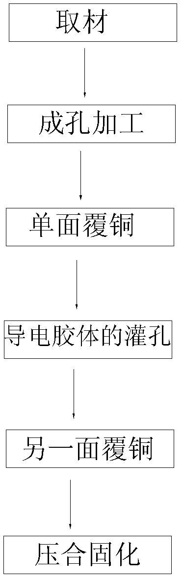
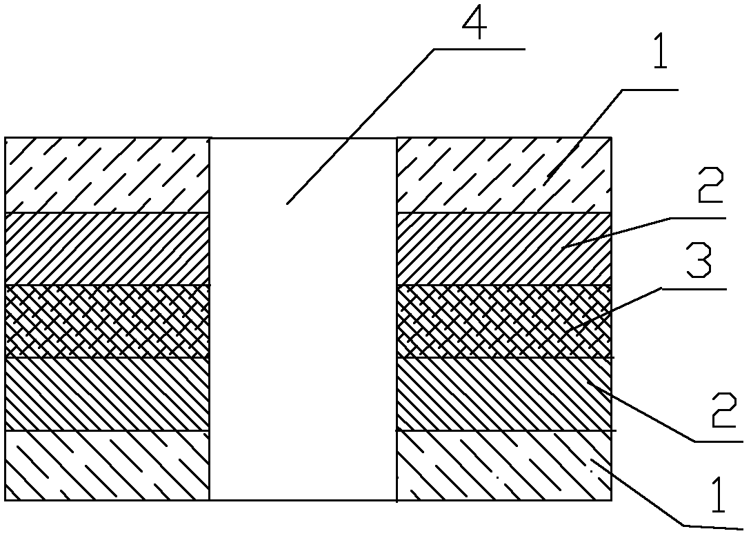
[0040] This embodiment provides a manufacturing process for interlayer copper connections of printed circuit boards, such as figure 2 shown, including the following steps:

[0041] Step 1: Take materials: Coat the adhesive resin layer on both sides of the outer surface of the insulating layer, and then glue and press the release paper on both sides of the outermost outer surface;

[0042] Take the insulating layer 3 made of glass fiber resin, with a thickness of 12.5 μm, and coat the adhesive resin layer 2 made of acrylic resin glue on the outer surface of the insulating layer 3. The thickness of the adhesive resin layer 2 is 10 μm, the speed of the coating machine is 4m / min, the temperature of the drying tunnel is 60°C, after preliminary drying in the drying tunnel, apply the adhesive resin layer 2 made of acrylic resin glue on the other side again, and repeat the previous coating operation The procedure is to stick and press the release paper 1 on the outer surface of the ...

Embodiment 2

[0060] This embodiment provides a manufacturing process for interlayer copper connections of printed circuit boards, such as figure 2 shown, including the following steps:

[0061] Step 1: Collect materials

[0062] Take the insulating layer 3 made of polyimide PI film, with a thickness of 200 μm, and coat the adhesive resin layer 2 made of modified acrylic resin glue on the outer surface of the insulating layer 3, the adhesive resin layer The thickness of 2 is 100 μm, the speed of the coating machine is 4m / min, and the temperature of the drying tunnel is 60°C. After preliminary drying in the drying tunnel, the adhesive resin layer 2 made of modified acrylic resin glue is coated again on the other side, and repeated In the previous coating operation procedure, the release paper 1 was glued and pressed on both sides of the outermost layer of the double-sided outermost layer, the pressure was 6MPa, and the temperature was 80°C.

[0063] Step 2: Hole forming;

[0064] Then ca...

Embodiment 3

[0079] This embodiment provides a manufacturing process for interlayer copper connections of printed circuit boards, such as figure 2 shown, including the following steps:

[0080] Step 1: Collect materials

[0081] Get the insulating layer 3 made of polyester PET film, its thickness is 80 μ m, the adhesive resin layer 2 that is made of epoxy resin glue is coated on the outer surface of the insulating layer 3, the adhesive resin layer 2 The thickness is 50μm, the speed of the coating machine is 4m / min, and the temperature of the drying tunnel is 60°C. After preliminary drying in the drying tunnel, the adhesive resin layer 2 made of epoxy resin glue is coated again on the other side, and the previous coating is repeated. Overlapping operation procedure, double-sided sticking and pressing release paper 1 on the outer surface of the double-sided outermost layer, the pressure is 6MPa, and the temperature is 80°C.

[0082] Step 2: Hole forming;

[0083] Drilling is then carried...


PUM

PropertyMeasurementUnit
Thicknessaaaaaaaaaa
Thicknessaaaaaaaaaa
Thicknessaaaaaaaaaa

Abstract

The invention discloses a manufacturing process of an interlayer copper connector of a printed circuit board. The manufacturing process comprises the following steps: coating a glue resin layer and sticking and pressing release paper on two sides of the outer surface of an insulation layer; forming pores and machining; removing the release paper on one side and coating a copper layer; filling holes with electric conductive colloid; removing the release paper on the other side and coating a copper layer; and pressing, fitting and curing. According to the invention, by adopting a simply and easily operated silk screen printing technology and by combining the electric conductive colloid with low liquidity, the chemical copper depositing and plating technology in the production technology of the traditional printed circuit board is replaced successfully, the conduction performance of the copper layer on performance can be achieved, zero emission and zero pollution in the environment protection aspect are achieved, the investment total amount in device input and plant input aspects is reduced, the investment hazard is reduced, and the conditions for rapid production and manufacturing cycle shortening are provided for the market demand of the printed circuit boards on the aspect of production efficiency.

Description


Claims


Application Information

Patent Timeline
Owner SHENZHEN HONGHAI ELECTRON MATERIAL TECH CO LTD
Why Eureka
Try Eureka