
Substrate processing apparatus, wafer holder, and method of manufacturing semiconductor device

一种衬底处理装置、晶片支架的技术,应用在半导体/固态器件制造、电气元件、电路等方向

Active Publication Date: 2016-05-11
KOKUSAI DENKI KK
View PDF6 Cites 0 Cited by
  • Summary
  • Abstract
  • Description
  • Claims
  • Application Information

AI Technical Summary

Problems solved by technology

It is conceivable to use a material with excellent heat resistance such as SiC to form a boat in which multiple parts are fixed as in the past, but materials such as SiC have good heat resistance, and accordingly it is difficult to fix them by welding or the like.

Method used


Image

  • Substrate processing apparatus, wafer holder, and method of manufacturing semiconductor device
  • Substrate processing apparatus, wafer holder, and method of manufacturing semiconductor device
  • Substrate processing apparatus, wafer holder, and method of manufacturing semiconductor device

Examples


no. 1 approach

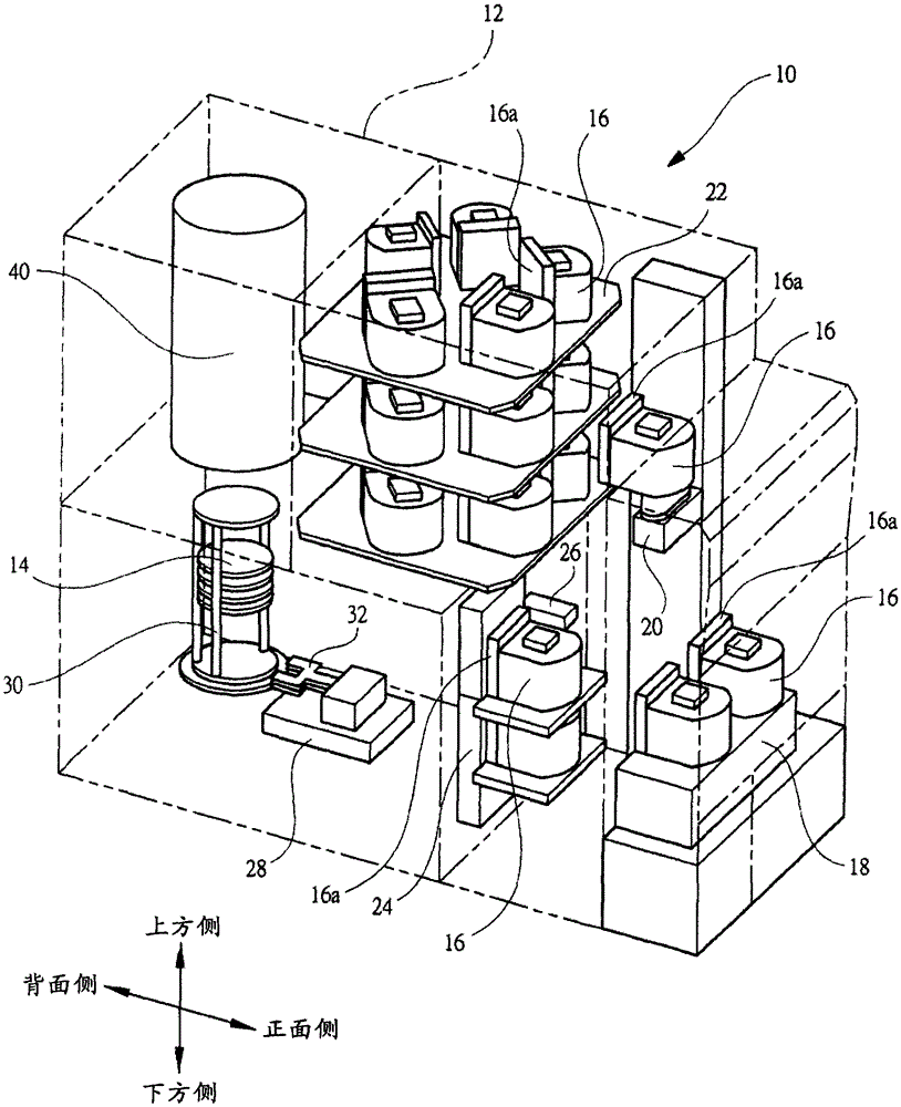
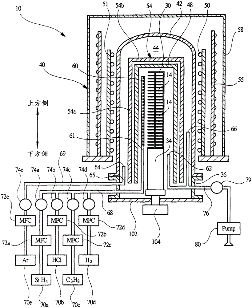
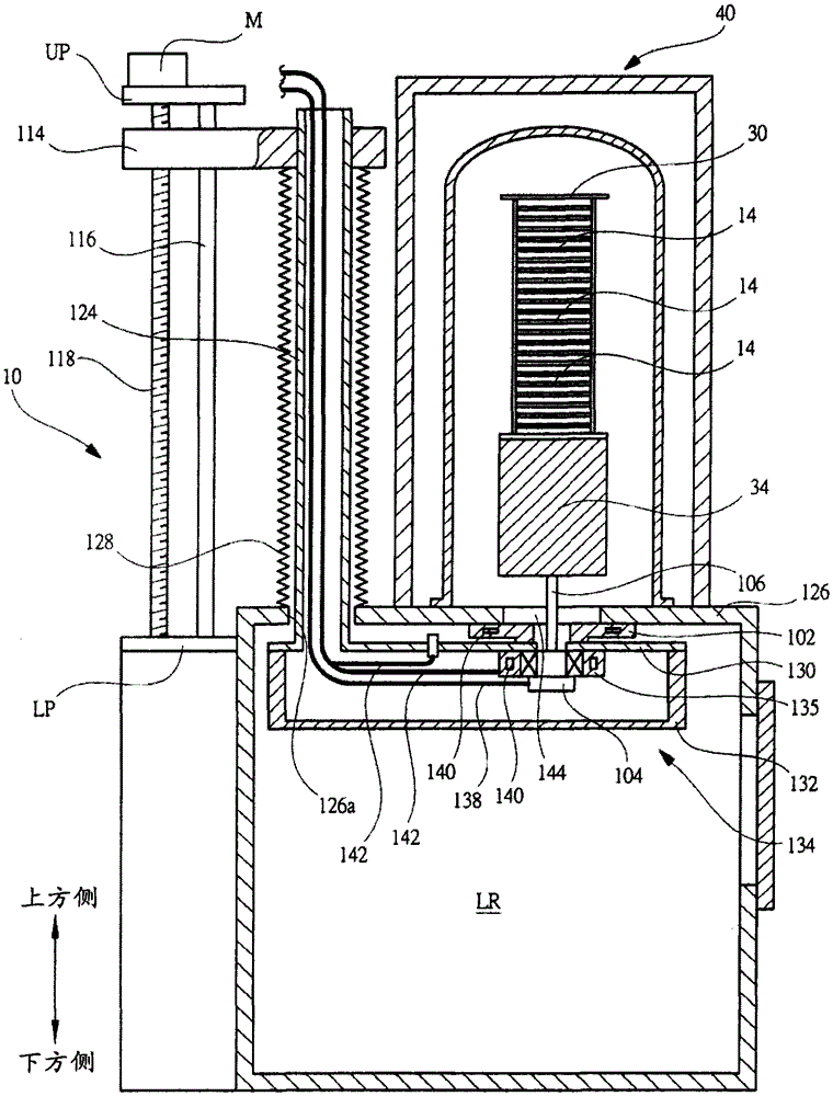
[0035] [First Embodiment] Hereinafter, a first embodiment of the present invention will be described in detail with reference to the drawings. In the following embodiments, a so-called batch type vertical SiC epitaxial growth apparatus that stacks SiC wafers in the height direction (vertical direction) is exemplified as a SiC epitaxial growth apparatus that is an example of a substrate processing apparatus. Thereby, the number of SiC wafers that can be processed at one time is increased and the throughput (manufacturing efficiency) is improved.

[0036] figure 1 It is a perspective view showing the outline of the substrate processing apparatus of the present invention. First, use figure 1 A substrate processing apparatus for forming an SiC epitaxial thin film and a method for manufacturing a substrate for forming an SiC epitaxial thin film, which is one of the manufacturing steps of a semiconductor device in one embodiment of the present invention, will be described.

[003...

no. 2 approach

[0122] [Second Embodiment] Hereinafter, a second embodiment of the present invention will be described in detail with reference to the drawings. In addition, about the same part as the said 1st Embodiment, the same code|symbol is attached|subjected, and the detailed description is abbreviate|omitted.

[0123] Figure 12 represent the wafer holder of the second embodiment and Figure 7 The corresponding stereogram, Figure 13 is for illustration Figure 12 An explanatory diagram of the reactive gas consumption portion of the wafer holder.

[0124] In the second embodiment, only the shape of the holder base 210 forming the wafer holder 200 is different from the first embodiment described above. That is, in the first embodiment, a pair of cutouts 112d are provided on the stand base 110 (refer to Figure 7 ), the outer peripheral side is non-circular, and in the second embodiment, each notch 112d is not provided on the stand base 210, but the outer peripheral side is circular...


PUM


Abstract

The present invention provides a substrate processing apparatus having a stacked structure of wafers that achieves high temperature resistance without adversely affecting film formation accuracy. Each boat post (31a to 31c) has a holder base (110) that holds the wafer (14) on the inner peripheral side, and a holder holding portion (HS) that holds the outer peripheral side of the holder base (110). The holder base ( The outer diameter of the wafer (110) is larger than the outer diameter of the wafer (14), and the holder base (110) is detachable from the holder holding part (HS). There is no need to fix the holder base (110) and each boat column (31a-31c) by welding or the like. The holder base (110) and each boat column (31a-31c) can be formed of SiC or the like, and the high temperature resistance effect can be easily achieved. The stacked structure of the wafers. In addition, since the wafer (14) can be separated from the boat posts (31a to 31c) through the holder base (110), adverse effects on film formation accuracy can be suppressed.

Description

technical field [0001] The present invention relates to a substrate processing device for processing a plurality of stacked substrates, a wafer holder, and a method for manufacturing a substrate or a semiconductor device, and more particularly to a substrate for forming a silicon carbide (SiC) epitaxial thin film on a substrate. A bottom processing device, a wafer holder, and a method for manufacturing a substrate or a semiconductor device. Background technique [0002] Silicon carbide (SiC) is attracting attention especially as an element material for power devices because of its higher dielectric strength and thermal conductivity than silicon (Si). On the one hand, SiC is known to be more difficult to manufacture a crystal substrate and a semiconductor device (semiconductor device) than Si because of its small impurity diffusion coefficient and the like. For example, the epitaxial film formation temperature of Si is about 900°C to 1200°C, and the epitaxial film formation ...

Claims


Application Information

Patent Timeline
Patent Type & Authority Patents(China)
IPC IPC(8): H01L21/673H01L21/205
CPCH01L21/67309H01L21/67757
Inventor 福田正直佐佐木隆史山口天和原大介
Owner KOKUSAI DENKI KK
Features
  • Generate Ideas
  • Intellectual Property
  • Life Sciences
  • Materials
  • Tech Scout
  • Unparalleled Data Quality
  • Higher Quality Content
  • 60% Fewer Hallucinations
Learn More