Silicon on insulator (SOI) metal oxide semiconductor (MOS) transistor

A transistor and active area technology, applied in semiconductor devices, electrical components, circuits, etc., can solve the problems of increasing parasitic capacitance and parasitic resistance, affecting device performance, etc., and achieve the effect of reducing lateral leakage current

Active Publication Date: 2012-09-12
INST OF MICROELECTRONICS CHINESE ACAD OF SCI
View PDF1 Cites 9 Cited by
  • Summary
  • Abstract
  • Description
  • Claims
  • Application Information

AI Technical Summary

Problems solved by technology

[0006] H-type gate SOI MOS devices have source-body, drain-body parasitic capacitances, and parasitic resistances. As L increases, parasitic capacitances and parasitic resistances increase, affecting device performance.

Method used


Image

  • Silicon on insulator (SOI) metal oxide semiconductor (MOS) transistor
  • Silicon on insulator (SOI) metal oxide semiconductor (MOS) transistor
  • Silicon on insulator (SOI) metal oxide semiconductor (MOS) transistor

Examples


Embodiment Construction

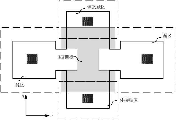
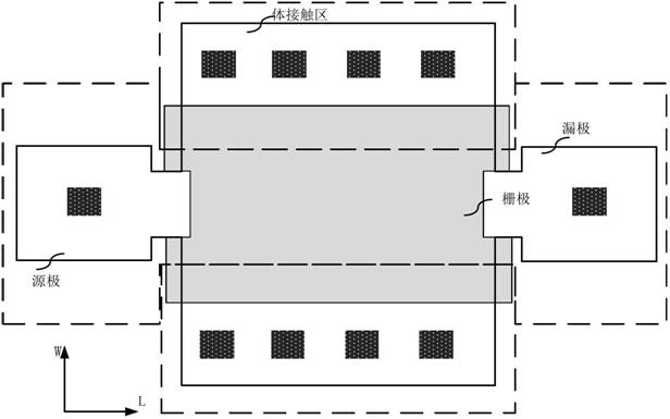
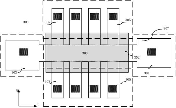
[0021] Embodiments of the invention are described in detail below, examples of which are illustrated in the accompanying drawings. The embodiments described below by referring to the figures are exemplary only for explaining the present invention and should not be construed as limiting the present invention.

[0022] The following disclosure provides many different embodiments or examples for implementing different structures of the present invention. To simplify the disclosure of the present invention, components and arrangements of specific examples are described below. Of course, they are only examples and are not intended to limit the invention. Furthermore, the present invention may repeat reference numerals and / or letters in different instances. This repetition is for the purpose of simplicity and clarity and does not in itself indicate a relationship between the various embodiments and / or arrangements discussed. In addition, various specific examples of processes and...


PUM


Abstract

The invention provides a silicon on insulator (SOI) metal oxide semiconductor (MOS) transistor, which comprises an active region formed in an SOI layer of an SOI substrate, a grid covering part of active region, a source region and a drain region, wherein the source region and the drain region are positioned in the active region on two sides of the grid in the length direction respectively; the width of the border part of the source region and the grid is the same as that of the border part of the drain region and the grid; the active region covered by the grid comprises a channel region which extends between the source region and the drain region at the width of the border part of the source region or the drain region and the grid; the active region comprises at least two comb-tooth-shaped bulges which are formed on one side or two sides of the channel region in the width direction at certain intervals along the length direction of the channel region; and part of the tail end of each comb-tooth-shaped bulge, which is not covered by the grid, is a bulk contact region. By the SOI MOS transistor, side electricity leakage, bulk resistance and parasitic capacitor can be reduced.

Description

technical field [0001] The invention relates to the field of semiconductor transistors, in particular to an SOI MOS transistor capable of suppressing the floating body effect of the SOI MOS (Metal Oxide Semiconductor) transistor. Background technique [0002] SOI (Silicon On Insulator) refers to silicon-on-insulator technology, and SOI technology is recognized as one of the mainstream semiconductor technologies in the 21st century. SOI technology effectively overcomes the shortage of bulk silicon materials, fully exploits the potential of silicon integrated circuit technology, and is gradually becoming the mainstream technology for manufacturing high-speed, low power consumption, high integration and high reliability VLSI. [0003] SOI MOS is divided into partially depleted SOI MOS (PDSOI) and fully depleted SOI MOS (FDSOI) according to whether the active body region is depleted. Generally speaking, the top silicon film of fully depleted SOI MOS is relatively thin, and the ...

Claims


Application Information

Patent Timeline
Patent Type & Authority Applications(China)
IPC IPC(8): H01L29/06H01L29/78
Inventor 李莹毕津顺罗家俊韩郑生
Owner INST OF MICROELECTRONICS CHINESE ACAD OF SCI
Why Eureka
Try Eureka