Preparation process of ridge waveguide DFB laser based on double-glue-layer structure

A DFB laser and ridge waveguide technology, which is applied to semiconductor lasers, lasers, laser components, etc., can solve the problems of difficulty in ensuring the consistency of chip production, difficulty in accurately controlling the depth of corrosion, and increase in leakage current. The effects of mass production, improved performance and reliability, and reduced failure rate

Pending Publication Date: 2020-12-04
武汉敏芯半导体股份有限公司
View PDF0 Cites 7 Cited by
  • Summary
  • Abstract
  • Description
  • Claims
  • Application Information

AI Technical Summary

Problems solved by technology

[0013] The following problems exist in the traditional process steps: the substrate to be coated with photoresist is a ridge waveguide structure with a certain depth, which makes it difficult for the photoresist to meet the requirements for flatness of the back surface of the waveguide structure. Resist requirements and overlay exposure technology requirements are relatively high
When using solution wet etching to develop and expose the photoresist layer, there is a certain relationship between the solution etching speed and the concentration, uniformity, and etching time of the etching solution, so it is difficult to accurately control the depth of etching, resulting in corroded photolithography. It is difficult to keep the depth of glue consistent, and then dry etch SiO 2 insulating layer, it is difficult to avoid SiO on the ridge sidewall 2 Etching, resulting in an increase in leakage current, making it difficult to guarantee the consistency of chip production, and the device may be broken down under working conditions
The insufficiency of the traditional process method leads to the instability of the laser manufacturing process, which seriously affects the performance, reliability and product yield of the DFB laser

Method used


Image

  • Preparation process of ridge waveguide DFB laser based on double-glue-layer structure
  • Preparation process of ridge waveguide DFB laser based on double-glue-layer structure
  • Preparation process of ridge waveguide DFB laser based on double-glue-layer structure

Examples


Embodiment Construction

[0045] In order to make the object, technical solution and advantages of the present invention clearer, the present invention will be further described in detail below in conjunction with the accompanying drawings and embodiments. It should be understood that the specific embodiments described here are only used to explain the present invention, not to limit the present invention.

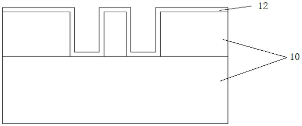
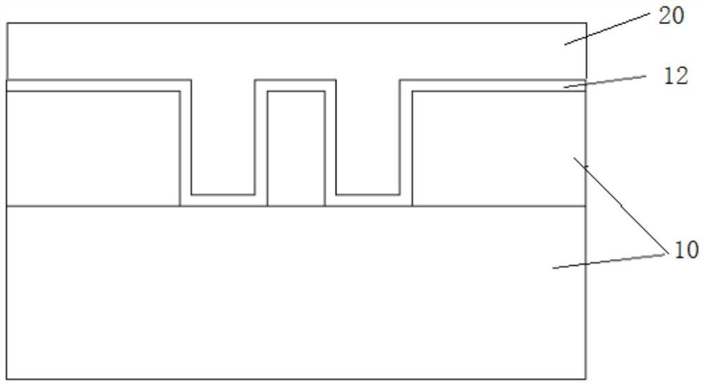
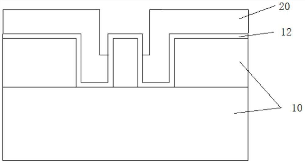
[0046] The preparation process of the ridge waveguide DFB laser based on the double glue layer structure in the embodiment of the present invention mainly includes several steps of material growth, grating preparation and burying, ridge waveguide preparation, ridge area current channel opening and electrode evaporation.

[0047] Such as Figure 5 As shown, the opening of the current channel in the ridge region specifically includes the following steps:

[0048] S1. Deposit a layer of SiO by plasma enhanced chemical vapor deposition 2 Insulation;

[0049] S2, in SiO 2 The surface of the insulati...


PUM

PropertyMeasurementUnit
thicknessaaaaaaaaaa

Abstract

The invention discloses a preparation process of a ridge-type waveguide DFB laser based on a double-glue-layer structure. Windowing of a ridge-type region current channelcomprises the steps: depositing a SiO2 insulating layer in a plasma enhanced chemical vapor deposition mode; coating a first layer of photoresist on the surface of the SiO2 insulating layer, and baking the first layer of photoresist to prevent the first layer of photoresist from being corroded by a wet method; coating a second layer of photoresist on the first layer of photoresist; baking the second layer of photoresist, wherein the baking temperature and time are both lower than those of the first layer of photoresist; performing exposure and development on the second layer of photoresist by using the photomask; corrodingthe second layer of photoresist subjected to exposure and development by adopting a wet etching process; etching the first layer of photoresist by adopting an RIE dry etching process; and etching theSiO2 insulating layer by adopting an RIE dry etching process, and removing the SiO2 insulating layer on the ridge strips to form a current channel. According to the method, the ridge-shaped structurewith a complete vertical shape on the side surface can be prepared.

Description

technical field [0001] The invention belongs to the technical field of semiconductor laser preparation technology, and relates to a preparation technology of a ridge waveguide DFB laser based on a double glue layer structure. Background technique [0002] In optical fiber communication, semiconductor lasers have become the core signal transmission source in the field of optical communication due to their small size, high efficiency, low power consumption, and easy integration. With the rapid development of optical fiber communication, long-wavelength DFB (Distributed Feedback Laser) lasers are widely used in high-speed transmission systems due to their stable dynamic single longitudinal mode characteristics. Especially in recent years, the rapid development of FTTH has greatly promoted the development of DFB laser epitaxy. Development of materials and process preparation processes. [0003] At present, there are two structures of DFB lasers, ridge waveguide structure (RWG) ...

Claims


Application Information

Patent Timeline
Patent Type & Authority Applications(China)
IPC IPC(8): H01L21/027H01L21/311H01S5/125H01S5/22
CPCH01L21/0273H01L21/0274H01L21/31116H01L21/31144H01S5/125H01S5/22
Inventor 王丹王权兵刘巍阳洪涛王任凡
Owner 武汉敏芯半导体股份有限公司
Why Eureka
Try Eureka