

ZnO and GaN-combined ZnO-based end surface transmitting laser and preparation method thereof
A surface-emitting laser and base-end technology, which is applied to the device for controlling the output parameters of the laser, the structure of the optical resonant cavity, etc., can solve the problems of low output power of the laser, poor laser directivity, and no controllable resonant cavity.
- Summary
- Abstract
- Description
- Claims
- Application Information
AI Technical Summary
Problems solved by technology
Method used
Image

Examples
Embodiment 1
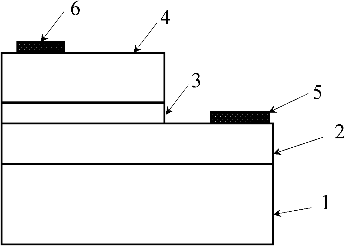
[0041] ZnO based end surface emitting lasers combining p-type ZnO and n-type GaN without current lower confinement layer. This ZnO-based end surface emitting laser combined with p-type ZnO and n-type GaN without a current lower confinement layer is shown in the appendix image 3 . The preparation process is as follows, taking the SiC crystal substrate as an example, using the n-type SiC crystal substrate as the substrate, and growing 1 to 10 microns of n-type ( Such as doped with Si)GaN epitaxial layer 2, the carrier concentration is 10 18 ~10 20 / cm 3 , and then adopt the MOCVD method, especially the special ZnO film growth MOCVD equipment described in No. 02100436.6 and ZL200410011164.0 patents to directly prepare the p-type ZnO-based material light-emitting layer 4 on the n-type GaN epitaxial layer 2, and the p-type ZnO-based material The thickness of the light-emitting layer 4 is 10 nanometers to 5 micrometers. The p-type preparation technology and p-type doping method...
Embodiment 2
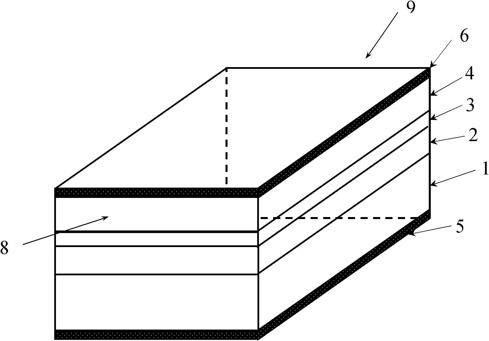
[0043] ZnO based end surface emitting lasers combining ZnO and GaN. This combined ZnO and GaN ZnO based end surface emitting laser is shown in the attached figure 2 , the chip is sequentially composed of substrate 1, p-type GaN epitaxial layer 2 prepared on substrate 1, Zn 1-x Mg x O (the value of x can be set between 0.05 and 1) the current lower confinement layer 3, the n-type ZnO-based material light-emitting layer 4 prepared on the current lower confinement layer 3, the upper electrode 6 prepared on the ZnO-based material light-emitting layer 4 The structure is characterized in that: the substrate 1 is a conductive GaAs crystal sheet, a conductive InP crystal sheet, a conductive SiC crystal sheet or a conductive GaN crystal sheet, and its conductivity type is the same as that of the GaN epitaxial layer 2. A lower electrode 5 is prepared under the bottom 1; a front reflector 8 and a rear reflector 9 are formed by the cleaved front and rear end faces of the chip, and the ...
Embodiment 3
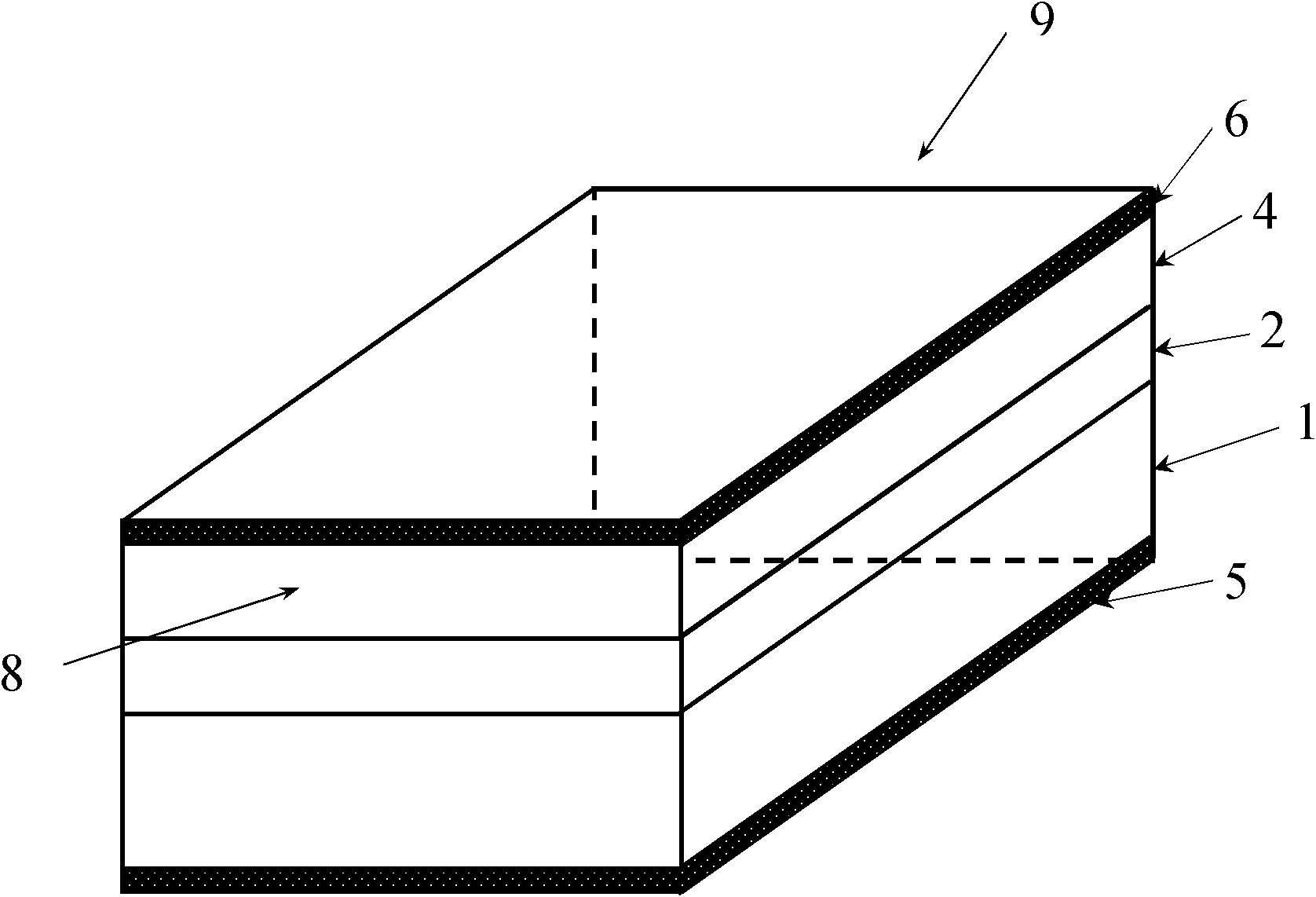
[0046] ZnO based end surface emitting lasers combining p-type ZnO and n-type GaN. This combination of p-type ZnO and n-type GaN ZnO-based end-surface-emitting lasers is still in the appendix figure 2 . The chip is sequentially composed of substrate 1, n-type GaN epitaxial layer 2 prepared on substrate 1, and GaN epitaxial layer prepared on epitaxial layer 2. 2 o 3 Or the n-type AlGaN current lower confinement layer 3, the p-type ZnO-based material luminescent layer 4 prepared on the current lower confinement layer 3, and the upper electrode 6 prepared on the ZnO-based material luminescent layer 4, characterized in that: the substrate 1 is conductive GaAs crystal sheet, conductive InP crystal sheet, conductive SiC crystal sheet or conductive GaN crystal sheet, its conductivity type is the same as that of GaN epitaxial layer 2, and a lower electrode 5 is prepared under the substrate 1 at the same time; The front and rear end faces of the chip cleavage form the front reflecto...
PUM
| Property | Measurement | Unit |
|---|---|---|
| thickness | aaaaa | aaaaa |
| thickness | aaaaa | aaaaa |
| thickness | aaaaa | aaaaa |
Abstract
Description
Claims
Application Information