Long wavelength GaNAsBi/GaAs multiple-quantum well laser and manufacturing method thereof

A technology of multiple quantum wells and multiple quantum well structures, applied in the field of semiconductor optoelectronics, can solve problems such as difficulties, and achieve the effects of low production cost, lower threshold current, and improved yield and lifespan

Active Publication Date: 2013-09-04
SUZHOU INST OF NANO TECH & NANO BIONICS CHINESE ACEDEMY OF SCI
View PDF3 Cites 6 Cited by
  • Summary
  • Abstract
  • Description
  • Claims
  • Application Information

AI Technical Summary

Problems solved by technology

So far, for the InGaNAs / GaAs material system, it is still difficult to increase the N component to 10%, and doping N atoms is easy to introduce defects, so the laser based on this material system is still in its infancy

Method used


Image

  • Long wavelength GaNAsBi/GaAs multiple-quantum well laser and manufacturing method thereof

Examples


Embodiment approach

[0059] As a preferred embodiment: the GaNAsBi / GaAs multi-quantum well contains 3 periods, GaAs is used as a barrier layer, GaNAsBi is used as a potential well layer, and a compressive strain of 1% is formed with GaAs, wherein the composition of N is 2.28% , the composition of Bi is 3.25%.

[0060] Preferably, the long-wavelength GaNAsBi / GaAs multi-quantum well laser is epitaxially grown on a GaAs substrate.

[0061] Preferably, the lower confinement layer is an N-type AlGaAs lower confinement layer, which is composed of an N-type AlGaAs layer, and the composition of Al is 15%.

[0062] Correspondingly, the upper confinement layer is a P-type AlGaAs upper confinement layer, which is composed of a P-type AlGaAs layer, and the composition of Al is 15%.

[0063] Correspondingly, the electron blocking layer is a P-type AlGaAs electron blocking layer, located between the AlGaAs upper waveguide layer and the upper confinement layer, and the composition of Al is 20%

[0064] Prefera...

Embodiment 1

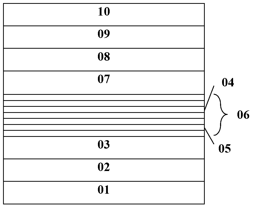
[0090] Embodiment one: if figure 1 , when using AlGaAs as the upper and lower confinement layers, the preparation method of the long-wavelength GaNAsBi / GaAs multi-quantum well laser comprises the following steps:

[0091] (1) grow described long-wavelength GaNAsBi / GaAs multiple quantum well laser with MOCVD method, its structure is as follows figure 1 Shown:

[0092] (1) N-type doping about 2×10 is grown on N-type GaAs substrate 01 18 cm -3 A 0.2 micron AlGaAs layer with an Al composition of 15% forms the lower confinement layer 02;

[0093] (2) grow a 0.1 micron non-doped AlGaAs layer with an Al composition of 8% to form the lower waveguide layer 03;

[0094] (3) Alternately grow 10nm GaAs barrier layer 04 (4 pieces) and 5.5nm GaNAsBi potential well layer 05 (3 pieces) with 1% compressive strain, in which the N component is about 2.28%, and the Bi component is about 3.25% , forming a 3-period multi-quantum well structure to form the active region 06 of the laser;

[009...

Embodiment 2

[0101] Embodiment 2: as figure 1 , when using GaInP as the upper and lower confinement layers, the preparation method of the long-wavelength GaNAsBi / GaAs multi-quantum well laser comprises the following steps:

[0102] (1) Growth of long-wavelength GaNAsBi / GaInP multi-quantum well laser by MOCVD method, its structure is as follows figure 1 Shown:

[0103] (1) On the N-type GaAs substrate 01 grow N-type doped about 2×10 18 cm -3 The 0.2 micron GaInP layer, the Al composition is 52%, forms the lower confinement layer 02;

[0104] (2) grow a 0.1 micron non-doped AlGaAs layer with an Al composition of 8% to form the lower waveguide layer 03;

[0105] (3) Alternately grow 10nm GaAs barrier layer 04 (4 pieces) and 5.5nm GaNAsBi potential well layer 05 (3 pieces) with 1% compressive strain, in which the N component is about 2.28%, and the Bi component is about 3.25% , forming a 3-period multi-quantum well structure to form the active region 06 of the laser;

[0106] (4) grow a ...


PUM


Abstract

The invention discloses a long wavelength GaNAsBi / GaAs multiple-quantum well laser, comprising a lower limit layer, a lower wave guide layer, an active region, an upper wave guide layer, an upper limit layer and an ohmic contact layer, which are connected in sequence, wherein the active region adopts a GaNAsBi / GaAs multiple-quantum well structure. According to the invention, the threshold current of the laser can be lowered, the gain of the laser can be increased, the refrigeration-free work can be realized, the laser is suitable for multiple lasers such as a surface launching laser, the production cost of the laser is far lower than that of an INP (indium phosphide)-based laser, no Al exists in the active region of the multiple-quantum well laser, the growth technics difficulty can be reduced, and the yield of the laser can be increased and the service life of the laser can be prolonged.

Description

【Technical field】 [0001] The invention relates to the field of semiconductor optoelectronics, in particular to a long-wavelength GaNAsBi / GaAs multi-quantum well laser and a preparation method thereof. 【Background technique】 [0002] Since the 1970s, optical fiber communication technology has developed rapidly, and semiconductor lasers as the best transmission light source occupy a very important position in it. Since the long-wavelength band of 1550nm corresponds to the lowest loss window of the optical fiber transmission system and is suitable for long-distance optical fiber communication, research on 1550nm semiconductor lasers is very active. [0003] At present, the commercialized 1550nm semiconductor lasers are mainly InGaAsP / InP and InAlGaAs / InP material systems. However, it is still difficult for InGaAsP / InP lasers to work at temperatures above 85°C without refrigeration. In order to meet the requirements of harsh ambient temperature (-25°C-85°C), complex and expens...

Claims


Application Information

Patent Timeline
Patent Type & Authority Applications(China)
IPC IPC(8): H01S5/343
Inventor 曾徐路董建荣李奎龙孙玉润于淑珍赵勇明赵春雨杨辉
Owner SUZHOU INST OF NANO TECH & NANO BIONICS CHINESE ACEDEMY OF SCI
Why Eureka
Try Eureka