Modulated doped multi-period strain-compensated quantum well epitaxial layer and its growth method

A strain compensation and modulation doping technology, which is applied in the direction of phonon exciters, laser components, semiconductor lasers, etc., can solve the problems affecting the luminous efficiency of quantum wells, lattice relaxation, and the quality of epitaxial growth of large strain multi-period quantum well materials Difficulties and other problems, to achieve the effect of improving external quantum efficiency, reducing Auger recombination, and increasing relaxation oscillation frequency

Active Publication Date: 2019-05-17
WUHAN HUAGONG GENUINE OPTICS TECH CO LTD
View PDF9 Cites 0 Cited by
  • Summary
  • Abstract
  • Description
  • Claims
  • Application Information

AI Technical Summary

Problems solved by technology

However, after increasing the strain of the well layer material in the active region of the quantum well, the stress caused by high mismatch can easily cause lattice relaxation, from two-dimensional growth to three-dimensional growth, and indium atoms are easy to migrate to form In-rich "islands". High-quality quantum wells require two-dimensional growth, because three-dimensional growth will cause many defects, which will affect the luminous efficiency of quantum wells
[0005] Due to the increased strain of the well layer material in the quantum well active region and multi-period accumulation, the overall strain of the quantum well active region is further increased, which brings difficulties to the quality of epitaxial growth of large strain and multi-period quantum well materials

Method used


Image

  • Modulated doped multi-period strain-compensated quantum well epitaxial layer and its growth method
  • Modulated doped multi-period strain-compensated quantum well epitaxial layer and its growth method
  • Modulated doped multi-period strain-compensated quantum well epitaxial layer and its growth method

Examples


Embodiment Construction

[0039] The present invention will be described in further detail below in conjunction with the accompanying drawings and embodiments. The following examples are used to illustrate the present invention, but should not be used to limit the scope of the present invention.

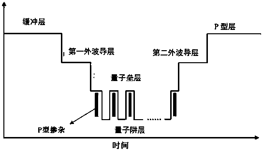
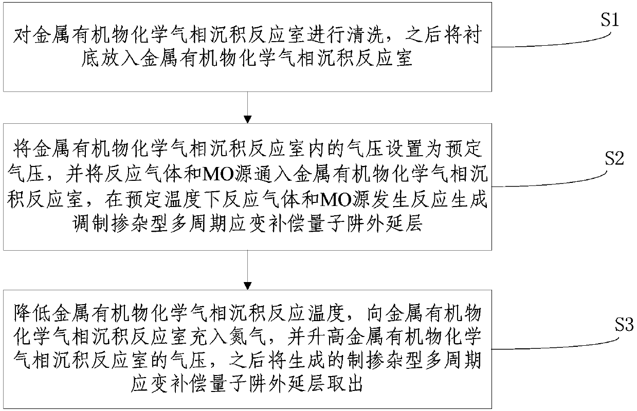
[0040] A modulation doped multi-period strain compensation quantum well epitaxial layer growth method, such as figure 1 As shown, the method includes the following steps:

[0041] S1. Baking and cleaning the metal-organic chemical vapor deposition MOCVD reaction chamber to remove foreign matter on the surface, and then placing the substrate on the base of the metal-organic chemical vapor deposition reaction chamber MOCVD; wherein the substrate is an InP substrate Bottom, the baking temperature is 740 degrees;

[0042] S2. Set the pressure in the metal-organic chemical vapor deposition reaction chamber to a predetermined pressure, and pass the reaction gas and the MO source into the metal-organic chemical va...


PUM


Abstract

The invention discloses a modulation-doped multi-period strain-compensated quantum well epitaxial layer and a growth method thereof. Air pressure in a metal organic chemical vapor deposition reaction chamber is set as predetermined air pressure and reaction gas and an MO source are piped into the metal organic chemical vapor deposition reaction chamber, and the reaction gas and the MO source react under predetermined temperature so as to generate the modulation-doped multi-period strain-compensated quantum well epitaxial layer, wherein the reaction gas is phosphorane and arsine; and the MO source is trimethylaluminum, trimethylindium, trimethylgallium, triethylgallium, P-type doped source dimethylzinc or P-type doped source diethylzinc. The modulation-doped multi-period strain-compensated quantum well epitaxial layer generated by the method is a high-linearity AlGaInAs quantum well epitaxial layer, and compressive strain is increased so that auger recombination and interband absorption can be reduced, and the effect of improving the high temperature characteristic of the device and the external quantum efficiency, the internal quantum efficiency and the conversion efficiency of an active area quantum well and enhancing relaxation oscillation frequency can be achieved.

Description

technical field [0001] The invention relates to the field of semiconductor lasers, in particular to a modulation doped multi-period strain compensation quantum well epitaxial layer and a growth method thereof. Background technique [0002] The semiconductor laser has developed from the initial operation at low temperature of 25°C to continuous operation at room temperature, and now it has developed to continuous operation at high temperature of 85°C. The active region of the semiconductor laser has developed from a homojunction to a single heterojunction, a double heterojunction, and a quantum well. (Single, multiple quantum wells) and other forms, in the final analysis, improve the external quantum efficiency, internal quantum efficiency and conversion efficiency of the semiconductor active layer material. [0003] In the prior art, the conduction band offset ΔEc=0.4ΔEg in the quantum well structure of AlGaInAs / InP material can only have a small electron confinement potenti...

Claims


Application Information

Patent Timeline
Patent Type & Authority Patents(China)
IPC IPC(8): H01S5/343
CPCH01S5/34366
Inventor 吴瑞华
Owner WUHAN HUAGONG GENUINE OPTICS TECH CO LTD
Why Eureka
Try Eureka