Super junction device and manufacturing method thereof

A super-junction device and manufacturing method technology, which is applied in semiconductor/solid-state device manufacturing, semiconductor devices, electrical components, etc., can solve the problems of increasing the difficulty of process control, large deviation of breakdown voltage, and increase of filling impurity concentration, etc., to achieve Effects of improving switch and body diode characteristics, increasing N impurity concentration, and increasing N-type doping concentration

Pending Publication Date: 2021-05-11
NANTONG SANRISE INTEGRATED CIRCUIT CO LTD
View PDF0 Cites 2 Cited by
  • Summary
  • Abstract
  • Description
  • Claims
  • Application Information

AI Technical Summary

Problems solved by technology

But in this way, in the manufacturing process, especially in the trench process, due to the small width of the P column, the difficulty of process control is increased, and at the same time, the concentration of filling impurities is increased, and because of the increase in the absolute value of the concentration, the same percentage of process Changes, the change of the total amount of impurities will increase, the degree of charge imbalance will be serious, and the deviation of device performance, including the deviation of breakdown voltage, will be large, affecting the consistency of the device

Method used


Image

  • Super junction device and manufacturing method thereof
  • Super junction device and manufacturing method thereof
  • Super junction device and manufacturing method thereof

Examples


no. 1 example

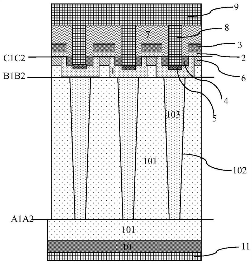
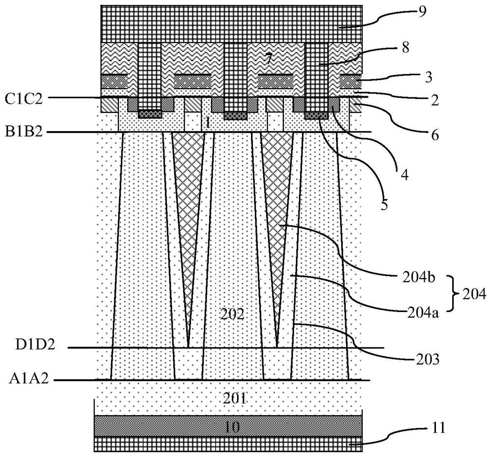
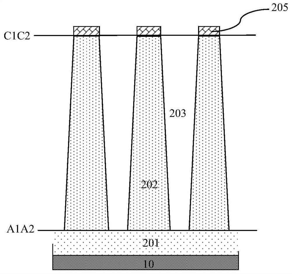
[0098] The first embodiment of the present invention can obtain the following beneficial technical effects:

[0099] 1. In the first embodiment of the present invention, the super-junction structure is specially set from the overall structure of the super-junction device. The width of the N-type column 204 and the volume of the N-type column 204 are increased under the condition of keeping the same to reduce the specific on-resistance of the super junction device; on this basis, the first embodiment of the present invention selects the N-type with a larger width The top width of the column 204 is used as the top opening width of the trench 203, and the N-type column 204 is set to be composed of the N-type epitaxial layer filled in the trench 203, that is, the second N-type epitaxial layer, and the trench 203 is formed The epitaxial layer is a P-type epitaxial layer, that is, the first P-type epitaxial layer. Since the width of the top opening of the trench 203 is increased, th...


PUM

PropertyMeasurementUnit
thicknessaaaaaaaaaa
electrical resistivityaaaaaaaaaa
thicknessaaaaaaaaaa

Abstract

The invention discloses a super junction structure, and the structure is formed above the surface of a first N-type epitaxial layer, wherein the width of a P-type column at the top position of a super junction unit is less than that of an N-type column and is unchanged in a step mode; the N-type column is composed of a second N-type epitaxial layer filling grooves, the P-type column is composed of a first P-type epitaxial layer between the grooves, and the first P-type epitaxial layer is formed on the first N-type epitaxial layer; the grooves penetrate through the first P-type epitaxial layer, and the bottoms of the grooves are in contact with the first N-type epitaxial layer; the total amount of P-type impurities of the P-type column in the super junction unit is matched with the total amount of N-type impurities of the N-type column, the second N-type epitaxial layer is formed by overlapping at least two N-type epitaxial sub-layers, and the doping concentration of the first N-type epitaxial sub-layer is higher than that of the P-type column. The invention further discloses a manufacturing method of the super junction device. According to the invention, the process control difficulty can be reduced, the charge balance of the super junction unit can be improved, the reverse recovery current of the body diode is reduced, and the high-temperature characteristic of the device is improved.

Description

technical field [0001] The invention relates to the field of manufacturing semiconductor integrated circuits, in particular to a super junction device; the invention also relates to a method for manufacturing the super junction device. Background technique [0002] A super junction structure is a structure of alternately arranged N-type pillars and P-type pillars, that is, PN pillars. If the superjunction structure is used to replace the N-type drift region in the vertical double-diffused MOS transistor (Vertical Double-diffused Metal-Oxide-Semiconductor, VDMOS) device, a conduction path is provided in the conduction state (only the N-type column provides a path, The P-type column is not provided), and bears the reverse bias voltage in the off state (the P and N columns are jointly borne), and a super-junction metal-oxide-semiconductor field-effect transistor (Metal-Oxide-Semiconductor Field-Effect Transistor, MOSFET) is formed. The super-junction MOSFET can greatly reduce ...

Claims


Application Information

Patent Timeline
Patent Type & Authority Applications(China)
IPC IPC(8): H01L29/06H01L29/78H01L21/336
CPCH01L29/0634H01L29/66712H01L29/7802
Inventor 肖胜安曾大杰
Owner NANTONG SANRISE INTEGRATED CIRCUIT CO LTD
Why Eureka
Try Eureka