Rapid superjunction longitudinal double-diffusion metal oxide semiconductor transistor

A technology of vertical double-diffusion and semiconductor tubes, which is applied in the direction of semiconductor devices, electrical components, circuits, etc., can solve the problems of increasing junction area, large reverse recovery charge, and restricting the reverse recovery characteristics of devices, so as to improve the withstand voltage performance , Improve the effect of horizontal pressure resistance

Inactive Publication Date: 2011-02-09
SOUTHEAST UNIV
View PDF3 Cites 31 Cited by
  • Summary
  • Abstract
  • Description
  • Claims
  • Application Information

AI Technical Summary

Problems solved by technology

[0003] However, referring to figure 2 , in traditional superjunction vertical double-diffused metal-oxide-semiconductor transistors, the junction area of ​​the body diode is significantly larger than that of the vertical double-diffused metal-oxide-semiconductor field effect transistor. A large number of minority carriers are injected into the side to store a large amount of charge, resulting in a lot of reverse recovery charges when the source and d

Method used


Image

  • Rapid superjunction longitudinal double-diffusion metal oxide semiconductor transistor
  • Rapid superjunction longitudinal double-diffusion metal oxide semiconductor transistor
  • Rapid superjunction longitudinal double-diffusion metal oxide semiconductor transistor

Examples


Embodiment Construction

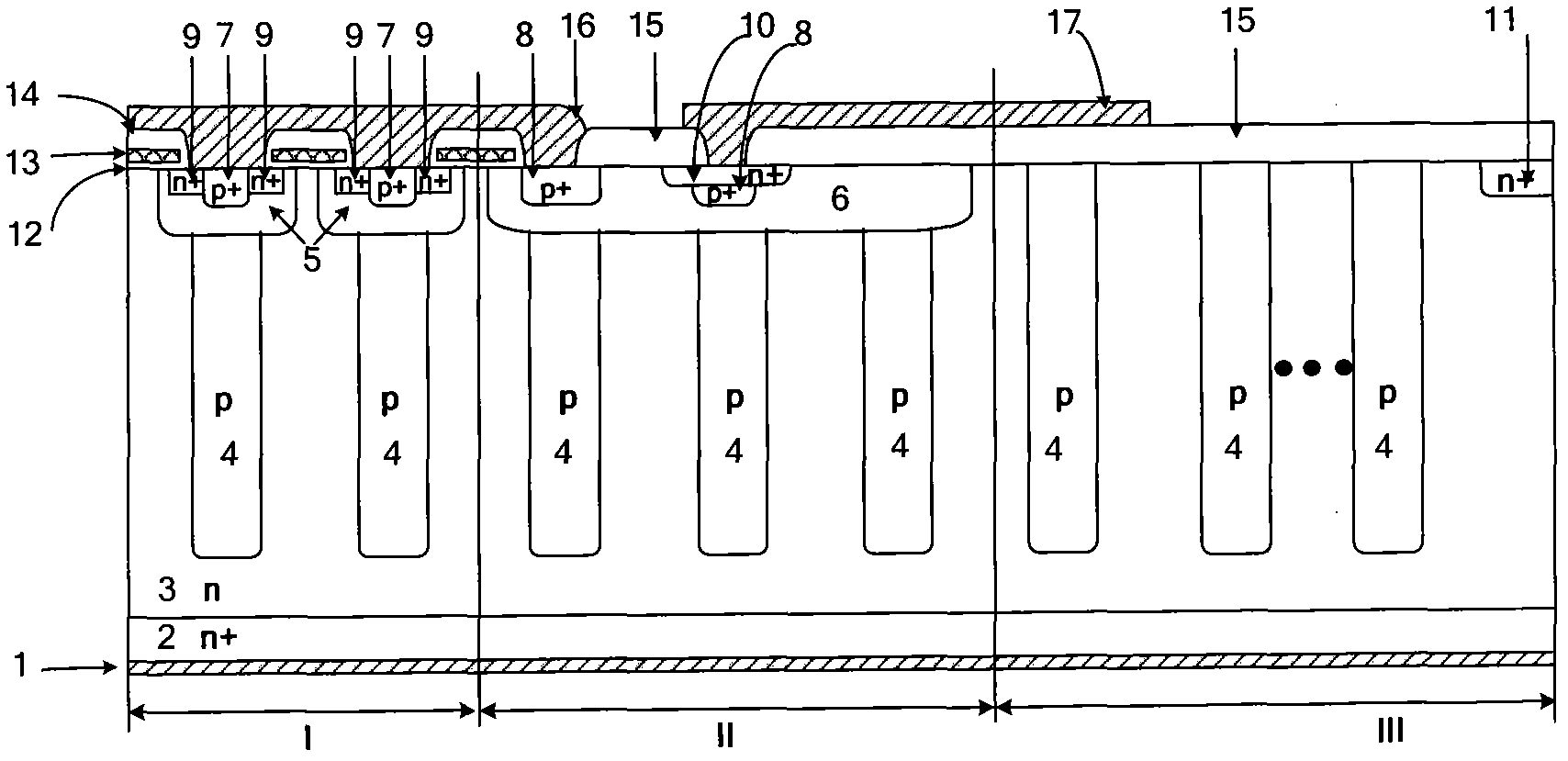
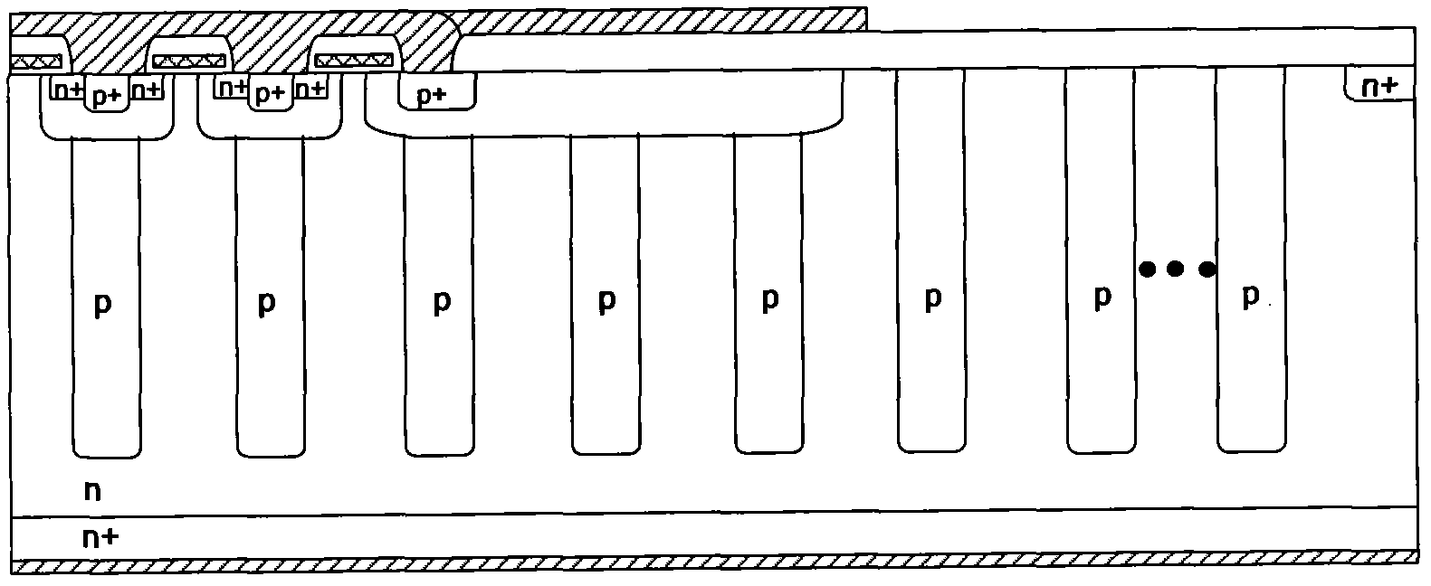
[0023] refer to figure 1 , a fast superjunction vertical double-diffused metal oxide semiconductor tube, comprising: a cell region I, a terminal region III located on the outermost periphery of the chip, and a transition region II between the cell region I and the terminal region III, in the cell region A drain metal 1 is provided at the bottom of the cell region I, transition region II and terminal region III, and a heavily doped n-type silicon substrate 2 is arranged on the drain metal 1 as the drain region of the chip. An n-type doped epitaxial layer 3 is arranged on the n-type silicon substrate 2, and a discontinuous p-type doped columnar semiconductor region 4 is arranged in the n-type doped epitaxial layer 3,

[0024] A first p-type doped semiconductor region 5 is provided on the p-type doped columnar semiconductor region 4 in the cell region 1, and the first p-type doped semiconductor region 5 is located in the n-type doped epitaxial layer 3. A p-type doped semiconduc...


PUM


Abstract

The invention relates to a rapid superjunction longitudinal double-diffusion metal oxide semiconductor transistor which comprises a cell area, a terminal area and a transition area, wherein the terminal area is arranged at the outermost periphery of a chip; the transition area is positioned between the cell area and the terminal area; the bottoms of the cell area, the transition area and the terminal area (III) are provided with drain electrode metal; a heavy doping n-type silicon substrate is arranged on the drain electrode metal and used as a drain area of the chip; an n-type doping epitaxial layer is arranged on the heavy doping n-type silicon substrate; and a discontinuous p-type doping columnar semiconductor area is arranged in the n-type doping epitaxial layer. The rapid superjunction longitudinal double-diffusion metal oxide semiconductor transistor is characterized in that an n-type heavy doping semiconductor area is arranged in a second p-type doping semiconductor area in the transition area, and the surface of the n-type heavy doping semiconductor area is provided with a contact hole which is connected with a metal layer to form a ground contact electrode of the chip. The invention can effectively reduce the reverse recovery charge of a device and improve the reverse recovery characteristics under the conditions of not increasing the process cost or changing the main parameter of the device.

Description

technical field [0001] The invention relates to a high-voltage power metal oxide semiconductor device made of silicon, more precisely, a high-voltage superjunction vertical double-diffused metal oxide semiconductor field effect transistor made of silicon. Background technique [0002] At present, power devices are more and more widely used in daily life, production and other fields, especially power metal oxide semiconductor field effect transistors, because they have faster switching speed, smaller drive current, and wider safe operating area , so it has been favored by many researchers. Nowadays, power devices are developing rapidly in the direction of increasing operating voltage, increasing operating current, reducing on-resistance and integration. Among many power MOSFET devices, especially in vertical power MOSFETs, the invention of super junction semiconductor power devices overcomes the on-resistance of traditional power MOSFETs The contradiction between the breakd...

Claims


Application Information

Patent Timeline
IPC IPC(8): H01L29/78H01L29/36H01L29/06H01L29/41
Inventor 钱钦松祝靖孙伟锋陆生礼时龙兴
Owner SOUTHEAST UNIV
Why Eureka
Try Eureka