Method of cross-point memory programming and related devices

a programming and memory technology, applied in the field of semiconductor memory devices, can solve the problems of difficult further scaling down memory devices, memory devices consume a relatively large amount of power, and their read/write speed is relatively slow

Inactive Publication Date: 2010-11-11
SAVRANSKY SEMYON D
View PDF0 Cites 31 Cited by
  • Summary
  • Abstract
  • Description
  • Claims
  • Application Information

AI Technical Summary

Benefits of technology

[0021]Broadly speaking, the embodiments of the present invention fill industry needs by providing methods for programming a cross-point memory.

Problems solved by technology

However, it is difficult to further scale down memory devices.
Further, memory devices consume a relatively large amount of power, and their read / program speed is relatively slow.
The main problems of the cross-point memories are quite high reset current Irst about 1 mA (for 90 nm memory device) that is necessary to heat up a region inside PCA 110 to a temperature above the melting temperature Tm.
Tight control of such devices in mass production is also difficult.
Such device cannot be effectively cooled during programming PCM into a reset state, and, as the result, PCA in their reset state is partially crystalline.
Therefore such PCM devices have small dynamic range of resistances and limited retention.
Although these solutions are valid they required to introduce new materials in CMOS process in addition to the active material 110 that can be very difficult.

Method used


Image

  • Method of cross-point memory programming and related devices
  • Method of cross-point memory programming and related devices
  • Method of cross-point memory programming and related devices

Examples


Embodiment Construction

[0040]Several exemplary embodiments of the invention will now be described in details with reference to the accompanying drawings shown in FIGS. 1-8.

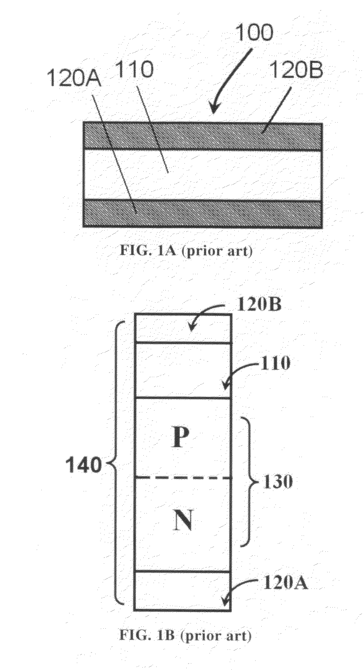
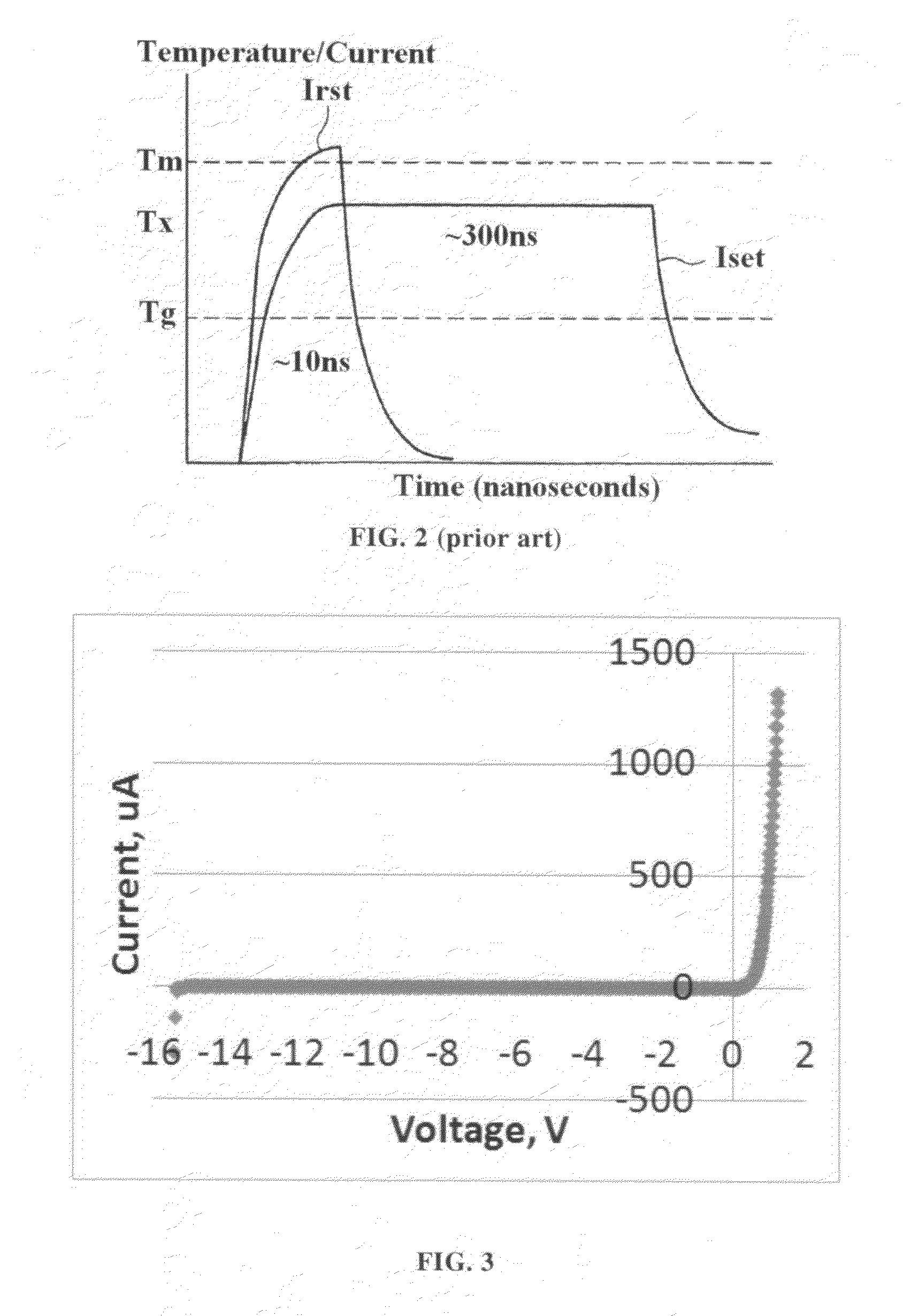
[0041]FIGS. 1-4 are explained in the background section of this invention. FIG. 5 shows a crossbar memory device 500 according to some embodiments of this invention and its electrical schematic. FIG. 6 shows examples of reverse recovery current pulses 600. FIG. 7 shows external signal pulses 700 applied to the memory device 500 in order to create various reverse recovery current pulses 600 needed to program the memory device 500 into one of non-volatile states.

[0042]A storage element 510 and a diode 530 electrically coupled in a crossbar memory device 500 as shown in FIG. 5. At least one of the storage element 510 or / and the diode 530 has finite (non-zero) reactance.

[0043]The storage element 510 is selected from the group consisting of a phase-change memory (PCM, PRAM, PCRAM, PC-RAM), a resistive memory (RRAM), a magnitoresistive memory...


PUM


Abstract

A reverse recovery current of a diode is used for programming a cross-point memory. Programming of a crossbar memory device, comprising a diode with preferably short charge carriers lifetime and a storage element by keeping the device at one polarity for a period of time and then switching it from first polarity to second polarity (e.g., forward to reverse polarity of the diode). Programming occurs due to diode's reverse recovery current. The value and duration of the recovery current pulse are selected to program the storage element into one of plurality of electrically distinguish states by variation of the level of current flowing through the device in the first polarity of applied bias voltage, by variation of the speed for changing the bias voltage from first polarity to second polarity, and by steady state value of the second polarity voltage applied to the device in one or more embodiments.

Description

CROSS REFERENCE TO RELATED APPLICATIONS[0001]This application claims priority to and the benefit of, and incorporates herein by reference in its entirety, U.S. Provisional Patent Application No. 61 / 215,473 which was filed on May 6, 2010.REFERENCE TO A SEQUENCE LISTING, A TABLE, OR A COMPUTER PROGRAM LISTING COMPACT DISK APPENDIX[0002]Not Applicable.REFERENCE REGARDING FEDERAL SPONSORSHIP[0003]Not Applicable.STATEMENT REGARDING FEDERALLY SPONSORED RESEARCH OR DEVELOPMENT[0004]Not Applicable.BACKGROUND OF THE INVENTION[0005]The present invention relates to semiconductor memory devices, and more particularly, to a cross-point memory programming.[0006]A variety of computer memory technologies are used to store computer programs and data. Examples of the computer memory technologies include a dynamic random access memory (DRAM), a static random access memory (SRAM), an erasable programmable read-only memory (EPROM), and an electrically erasable programmable read-only memory (EEPROM). Som...

Claims


Application Information

Patent Timeline
Patent Type & Authority Applications(United States)
IPC IPC(8): G11C11/00
CPCG11C11/5678G11C13/0004G11C13/0007G11C13/0011G11C2213/72G11C13/0069G11C2013/0073G11C2013/0078G11C2013/0092G11C13/0014
Inventor SAVRANSKY, SEMYON D.
Owner SAVRANSKY SEMYON D
Why Eureka
Try Eureka