

AlGaN-based double-channel Schottky diode based on groove anode structure and preparation method
A Schottky diode and anode structure technology, which is applied in semiconductor/solid-state device manufacturing, electrical components, circuits, etc., can solve problems such as limiting the application of GaN Schottky diodes and reducing the mobility of AlGaN/GaN heterostructures
- Summary
- Abstract
- Description
- Claims
- Application Information
AI Technical Summary
Problems solved by technology
Method used
Image

Examples
Embodiment 1
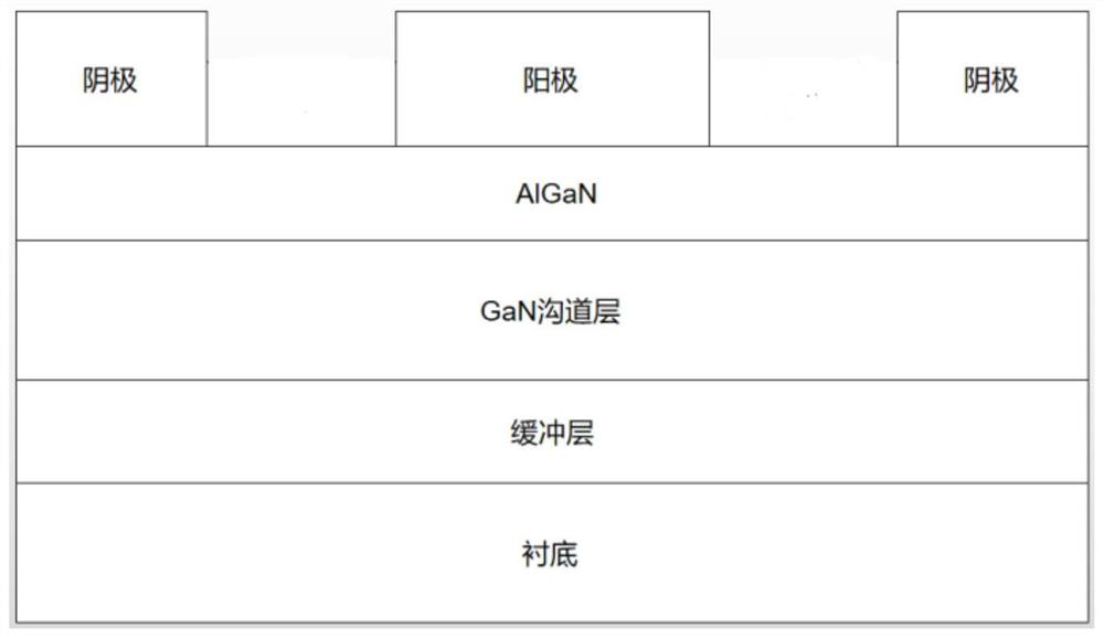
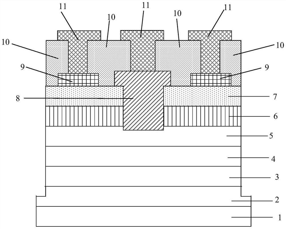
[0040] See figure 2 , figure 2It is a structural schematic diagram of an AlGaN-based dual-channel Schottky diode based on a recessed anode structure provided by an embodiment of the present invention. As shown in the figure, the AlGaN-based double-channel Schottky diode based on the recessed anode structure of this embodiment includes: a substrate 1, a buffer layer 2, a channel layer 3, a first barrier layer 4, a superlattice layer 5, second barrier layer 6, GaN cap layer 7, anode 8 and cathode 9. Wherein, the substrate 1 , the buffer layer 2 , the channel layer 3 , the first barrier layer 4 , the superlattice layer 5 , the second barrier layer 6 and the GaN cap layer 7 are stacked sequentially from bottom to top. The anode 8 is disposed on the GaN cap layer 7 , and its bottom passes through the GaN cap layer 7 and the second barrier layer 6 in turn, and is located in the superlattice layer 5 . The cathode 9 is disposed on the GaN cap layer 7 and surrounds the anode 8 , a...
Embodiment 2
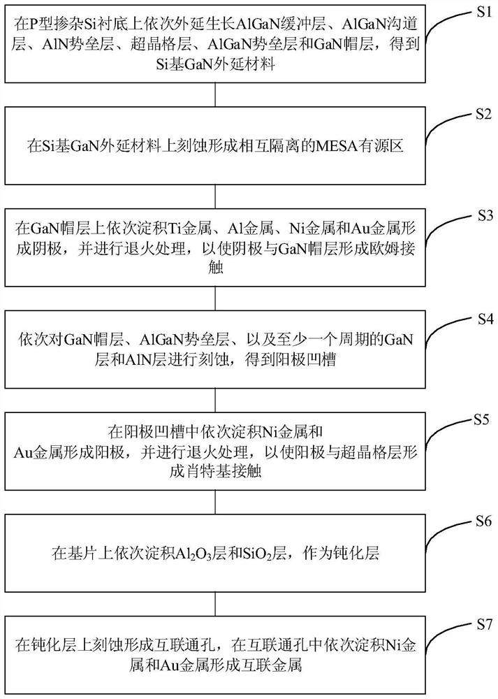
[0057] This embodiment provides a method for manufacturing an AlGaN-based dual-channel Schottky diode based on a recessed anode structure, which is applicable to the AlGaN-based dual-channel Schottky diode based on a recessed anode structure in the above embodiment. See image 3 , image 3 It is a flowchart of a method for preparing an AlGaN-based dual-channel Schottky diode based on a recessed anode structure provided by an embodiment of the present invention. As shown in the figure, the method of this embodiment includes:
[0058] S1: AlGaN buffer layer, AlGaN channel layer, AlN barrier layer, superlattice layer, AlGaN barrier layer and GaN cap layer are epitaxially grown on a P-type doped Si substrate in sequence to obtain a Si-based GaN epitaxial material, wherein , the superlattice layer includes GaN layers and AlN layers periodically arranged from bottom to top;
[0059] S2: Etching on the Si-based GaN epitaxial material to form mutually isolated MESA active regions; ...
PUM
| Property | Measurement | Unit |
|---|---|---|
| Thickness | aaaaa | aaaaa |
| Thickness | aaaaa | aaaaa |
| Thickness | aaaaa | aaaaa |
Abstract
Description
Claims
Application Information