A Vertical Cavity Surface Emitting Laser with Circular Spot

A vertical cavity surface emission, laser technology, applied in the direction of lasers, laser components, semiconductor lasers, etc., can solve the problems of device repeatability and uncontrollable yield, complex manufacturing process, large series resistance, etc., to improve the highest operation Power and reliability, large mode gain loss difference, and the effect of reducing leakage current

Active Publication Date: 2022-03-11
福建慧芯激光科技有限公司
View PDF0 Cites 0 Cited by
  • Summary
  • Abstract
  • Description
  • Claims
  • Application Information

AI Technical Summary

Problems solved by technology

This type of method needs to reduce the diameter of the oxidation hole of the device to 3-5 μm, the preparation process is very complicated, and the repeatability and yield of the device are relatively uncontrollable
At the same time, smaller oxidized pore size will bring problems such as large series resistance, severe heat generation, and poor stability.

Method used


Image

  • A Vertical Cavity Surface Emitting Laser with Circular Spot
  • A Vertical Cavity Surface Emitting Laser with Circular Spot
  • A Vertical Cavity Surface Emitting Laser with Circular Spot

Examples


Embodiment 1

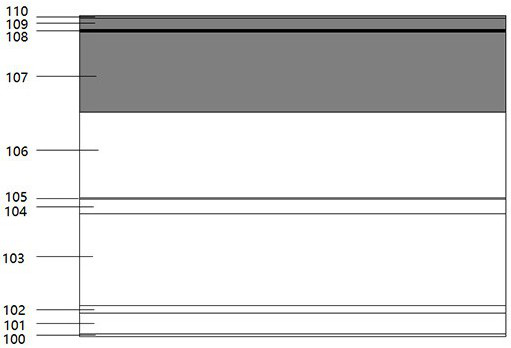
[0077] like figure 2 As shown, this embodiment provides a vertical cavity surface emitting laser with a circular spot, including a horizontal cavity laser unit, which includes an n-type contact metal layer 100, an n-GaAs Substrate 101, n-GaAs buffer layer 102, GaInP outer waveguide layer 103, first n-In x Ga 1-x As y P 1-y Lower waveguide layer 104, GaInP / In x Ga 1-x As y P 1-y / GaInP grating layer 105, second n-In x Ga 1-x As y P 1-y The lower waveguide layer 106, the third n-In x Ga 1- x As y P 1-y Lower waveguide layer 107, active layer 108, p-In x Ga 1-x As y P 1-y The upper waveguide layer 109 , the p-type contact layer 110 and the p-type contact metal layer 111 .

[0078] like figure 2 As shown, preferably, the thickness of the GaInP outer waveguide layer 103 is 3200 nm, which is used to confine the optical field.

[0079] like figure 2 Shown, preferably, GaInP / In x Ga 1-x As y P 1-y / GaInP grating layer 105 is GaInP layer, In x Ga 1-x As ...

Embodiment 2

[0097] like Figure 10 As shown, this embodiment discloses another vertical cavity surface emitting laser with a circular spot, which includes a horizontal cavity laser unit, and the horizontal cavity laser unit includes n-type contact metal layers 300, n -GaAs substrate 301, n-GaAs buffer layer 302, GaInP outer waveguide layer 303, n-In x Ga 1-x As y P 1-y Lower waveguide layer 304, active layer 305, first p-In x Ga 1-x As y P 1-y The upper waveguide layer 306, the second p-In x Ga 1-x As y P 1-y The upper waveguide layer 307, the third p-In x Ga 1-x As y P 1-y The upper waveguide layer 308 , the p-type contact layer 309 , and the p-type contact metal layer 310 .

[0098] like Figure 10 As shown, preferably, the layer thickness of the GaInP outer waveguide 303 is 2500 nm, which is used to confine the optical field.

[0099] like Figure 10 shown, preferably, n-In x Ga 1-x As y P 1-y The bandgap wavelength of the lower waveguide layer 304 is 870nm, the t...

Embodiment 3

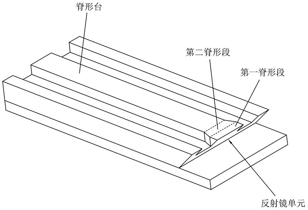
[0112] like Figure 14 As shown, the width of the second ridge section in this embodiment gradually increases from the upper ridge to the lower ridge, and the two side walls are curved. It can be seen from this that the plan view of the second ridge section is roughly arc-shaped. In addition, the technical features such as the specific structure of the horizontal resonator laser unit and the parameters of the rib region in this embodiment can be implemented by referring to the first or second embodiment, and will not be repeated here.


PUM

PropertyMeasurementUnit
thicknessaaaaaaaaaa
thicknessaaaaaaaaaa
thicknessaaaaaaaaaa

Abstract

The invention discloses a vertical-cavity surface-emitting laser with a circular light spot, which comprises a horizontal resonant cavity laser unit. The horizontal resonant cavity laser unit is etched with a double-groove structure on its surface, and a ridge is formed between the double-groove structures. A flat plate layer is formed under the double-groove structure; a mirror unit is etched obliquely at the end of the horizontal resonator laser unit in the laser emission direction. The etching angle θ of the mirror unit is 45°, and the etching depth is from horizontal to horizontal. The resonator laser unit starts from the surface and extends down to at least the bottom of the slab layer; the ridge platform is provided with an expanded horn section at one end close to the reflector unit. The reflector unit of the present invention can effectively transform the horizontal edge emitting beam into a vertical emitting beam, thereby facilitating the realization of a circular spot single-mode high-power vertical emitting, and overcomes the need to oxidize the aperture in order to achieve single-mode high power in the prior art Minimize the various problems that arise.

Description

technical field [0001] The invention relates to the technical field of semiconductor optoelectronics, in particular to a vertical cavity surface emitting laser with a circular light spot. Background technique [0002] Vertical cavity surface emitting laser (VCSEL) is widely used in optical communication, optical interconnection, optical It has a wide range of applications in neutral network and optical signal processing. The single transverse mode of a VCSEL is essential for most applications as it facilitates efficient coupling to fibers and eliminates noise and instabilities due to mode competition. [0003] In the laser resonator, the stable field distribution on a certain cross-section perpendicular to the propagation direction is called the transverse mode, that is, the light intensity distribution on the cross-section. Due to the fact that the reflective surface and the active area of ​​the laser are not ideal planes and the influence of the injected current, the act...

Claims


Application Information

Patent Timeline
Patent Type & Authority Patents(China)
IPC IPC(8): H01S5/065H01S5/183H01S5/22
CPCH01S5/18352H01S5/18361H01S5/18302H01S5/18308H01S5/22H01S5/0655
Inventor 鄢静舟薛婷杨奕祁鲁汉缪笛王坤
Owner 福建慧芯激光科技有限公司
Why Eureka
Try Eureka