Making method of electrical absorption modulation tunneling injection type distributed feedback semiconductor laser

A technology of electro-absorption modulation and distributed feedback, which is applied to semiconductor lasers, devices for controlling output parameters of lasers, lasers, etc., can solve problems such as high technological level requirements, influence, and quantum well thickness, so as to improve the characteristic temperature and eliminate the influence , high reliability effect

Inactive Publication Date: 2012-08-22
INST OF SEMICONDUCTORS - CHINESE ACAD OF SCI
View PDF7 Cites 0 Cited by
  • Summary
  • Abstract
  • Description
  • Claims
  • Application Information

AI Technical Summary

Problems solved by technology

[0004] The direct docking method can independently optimize the materials of the laser and the modulator, but requires two epitaxy active regions, which requires a higher level of technology; the selective area epitaxy method can obtain the active region of the laser and the modulator by epitaxy of the quantum well material at one time , but the quantum well in the laser part is thicker than the modulator region, which affects the extinction ratio performance of the modulator
And because both of these two growth methods introduce a dielectric film during the growth of the active region, it will adversely affect the life and reliability of the device

Method used


Image

  • Making method of electrical absorption modulation tunneling injection type distributed feedback semiconductor laser
  • Making method of electrical absorption modulation tunneling injection type distributed feedback semiconductor laser
  • Making method of electrical absorption modulation tunneling injection type distributed feedback semiconductor laser

Examples


Embodiment Construction

[0027] In order to make the object, technical solution and advantages of the present invention clearer, the present invention will be described in further detail below in conjunction with specific embodiments and with reference to the accompanying drawings.

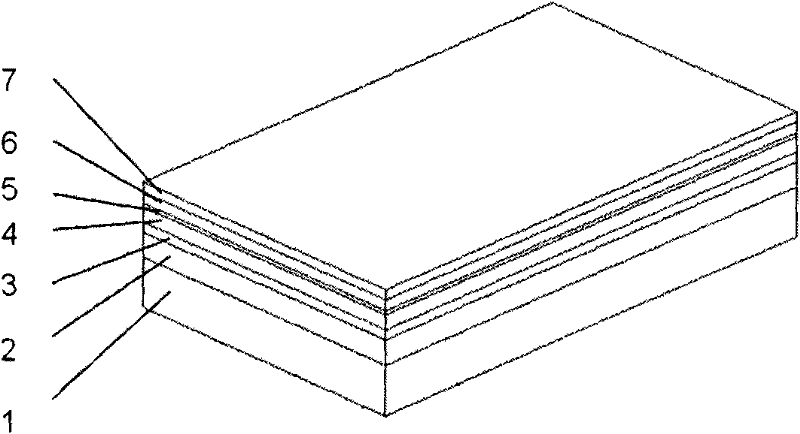
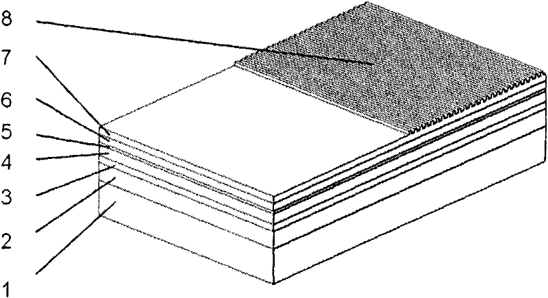
[0028] The present invention proposes a novel electroabsorption modulation distribution feedback semiconductor laser, which adopts a tunneling injection laser structure, uses the inner confinement layer of the lower waveguide as the main light absorption region of the modulator, can relatively independently optimize the performance of the laser and the modulator, and only needs One-time epitaxy of the active region, the process is simple and reliable, and the cost is low.

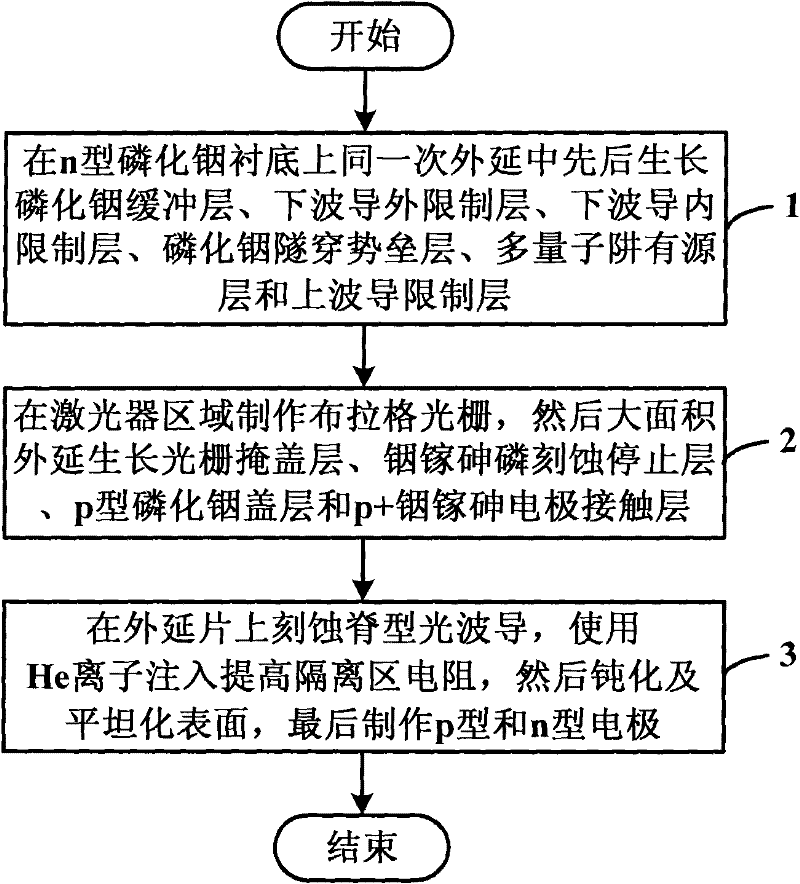
[0029] Such as figure 1 as shown, figure 1 It is a flowchart of a method for manufacturing an electroabsorption modulation tunneling injection distributed feedback semiconductor laser provided by the present invention, and the method includes the foll...


PUM


Abstract

The invention discloses a making method of an electrical absorption modulation tunneling injection type distributed feedback semiconductor laser, which comprises the following steps of: 1, growing an n-type indium phosphide buffer layer, a lower waveguide external limit layer, a lower waveguide internal limit layer, an indium phosphide tunneling barrier layer, a multiple quantum well active layerand an upper waveguide limit layer on an n-type indium phosphide substrate during the same epitaxy; 2, making a Bragg grating in a laser region, then epitaxially growing a p-type indium phosphide grating covering layer, an InGaAsP etching stopping layer, a p-type indium phosphide covering layer and a p+ InGaAs electrode contact layer largely; and 3, etching a ridge type optical waveguide on an epitaxial wafer, injecting with He ions to improve the resistance of an isolation region, and then passivating and flatting the surface and finally making a p-type and an n-type electrodes. The invention has the advantages of simple process and high reliability, eliminates the influence of hot electrons on the property of the laser, improves the characteristic temperature of the laser, and can realize a certain independent optimization on the laser and a modulator.

Description

technical field [0001] The invention relates to the technical field of semiconductor lasers, in particular to a manufacturing method of an electroabsorption modulation tunneling injection type distributed feedback semiconductor laser. Background technique [0002] In long-distance high-speed optical fiber communication systems, high-speed light sources will become the key components. Electroabsorption modulation distributed feedback semiconductor lasers have become promising high-speed light sources due to their small size, low chirp and many other advantages. [0003] Since the manufacture of electro-absorption modulation distributed feedback semiconductor lasers needs to integrate the laser and the modulator on the same substrate, and the functions of the laser and the modulator are different, the applicable material structure is quite different, so in order to make this integrated device, people have developed many Integration methods mainly include: direct docking metho...

Claims


Application Information

Patent Timeline
Patent Type & Authority Patents(China)
IPC IPC(8): H01S5/125H01S5/343H01S5/06
Inventor 汪洋赵玲娟朱洪亮王圩
Owner INST OF SEMICONDUCTORS - CHINESE ACAD OF SCI
Why Eureka
Try Eureka