Improvement method for stacked package of three-dimensional chip of microsystem

A three-dimensional chip, stacked packaging technology, applied in the direction of semiconductor/solid-state device components, semiconductor devices, electrical components, etc., can solve the problems of heat, stress, low integration density, etc., to reduce stress problems, reduce thermal stress problems, The effect of interconnecting high performance

Inactive Publication Date: 2016-03-23
CENT SOUTH UNIV
View PDF5 Cites 7 Cited by
  • Summary
  • Abstract
  • Description
  • Claims
  • Application Information

AI Technical Summary

Problems solved by technology

[0005] The present invention proposes a packaging method that uses a silicon-based adapter board to fundamentally solve the problems of heat, stress, and low integration density faced by traditional PCB board integration.

Method used


Image

  • Improvement method for stacked package of three-dimensional chip of microsystem

Examples


Embodiment Construction

[0020] The present invention will be further described below in conjunction with the accompanying drawings and embodiments.

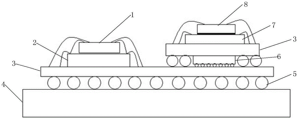
[0021] Such as figure 1 As shown, an improved method for microsystem three-dimensional chip stack packaging, the specific steps are as follows:

[0022] 1) First, according to the needs of microsystem packaging applications, design the redistribution layer and TSV layout on the silicon interposer A to realize the interconnection between devices;

[0023] 2) Mount the ASIC device and execution / sensor device on the adapter base with a placement machine, and use a wire bonding machine to complete the interconnection between ASIC and execution / sensor, and ASIC / execution / sensor and adapter board;

[0024] 3) According to the requirements of data and signal processing, design the redistribution layer and TSV layout of the silicon-based interposer B;

[0025] 4) Mount the memory device on the adapter board with a mounter, and complete the interconnection bet...


PUM


Abstract

The invention discloses an improvement method for stacked package of a three-dimensional chip of a microsystem. According to the improvement method, an application specific integrated circuit (ASIC) chip and an application processor are fixed on a traditional substrate by a silica-based transition board, the problems of difficulty in heat dissipation, stress damage, low integration density and the like faced by the traditional substrate can be fundamentally solved. With the improvement method disclosed by the invention, the silica-based transition board is simply and ingeniously applied to microsystem package, the influence of package stress on the microsystem performance is substantially eliminated, and interconnection with super-high density and calculation and storage capabilities with high performance are achieved.

Description

technical field [0001] The invention belongs to the field of microelectronic packaging, and relates to an improved method for microsystem three-dimensional chip stack packaging. Background technique [0002] Microsystem packaging is the process of mixing bare chips and devices with different functions in one package through micro-interconnection technology, and at the same time leading out I / O terminals to achieve mechanical connection to form a multi-functional integrated system. 60-80% of the cost is an important part of microsystems fabrication. At present, microsystem packaging mainly adopts three-dimensional stacked packaging technology based on PCB, metal or ceramic substrates, which can be roughly divided into stacked chip packaging and stacked package packaging. Compared with two-dimensional packaging, these methods have the advantages of small size, light weight, high silicon chip usage efficiency, and short signal delay. But the disadvantages are also obvious: 1)...

Claims


Application Information

Patent Timeline
Patent Type & Authority Applications(China)
IPC IPC(8): H01L25/16H01L23/538
CPCH01L23/5383H01L23/5385H01L25/162H01L2924/15311H01L2924/15331H01L2224/16227H01L2224/32145H01L2224/48091H01L2224/48145H01L2224/48227H01L2224/73265H01L2924/00014H01L2924/00012
Inventor 王福亮王峰朱文辉李军辉韩雷
Owner CENT SOUTH UNIV
Why Eureka
Try Eureka