Laser active region, semiconductor laser and manufacturing method thereof

A manufacturing method and laser technology, which are applied to semiconductor lasers, lasers, laser parts, etc., can solve the problems of easy introduction of defects, difficulties, and no refrigeration work when doped with N atoms, and achieve a large conduction band step ratio and electric field distribution. The effect of smoothing, improving slope efficiency

Active Publication Date: 2016-01-27
苏州市吴中中科育成科技发展有限公司
View PDF6 Cites 0 Cited by
  • Summary
  • Abstract
  • Description
  • Claims
  • Application Information

AI Technical Summary

Problems solved by technology

[0003] At present, the commercialized 1310nm semiconductor laser is mainly based on the InGaAsP / InP material system. However, it is still difficult for the InGaAsP / InP laser to work at a temperature above 85°C without refrigeration.
In order to solve this problem, another alternative material system that covers the optical band centered at 1310nm is being developed is InGaNAs / GaAs. So far, it is still difficult to increase the N component to 10% for the InGaNAs / GaAs material system. And doping N atoms is easy to introduce defects, so the laser based on this material system is still in its infancy

Method used


Image

  • Laser active region, semiconductor laser and manufacturing method thereof
  • Laser active region, semiconductor laser and manufacturing method thereof

Examples


Embodiment Construction

[0038] The present invention will be further described below with reference to the accompanying drawings.

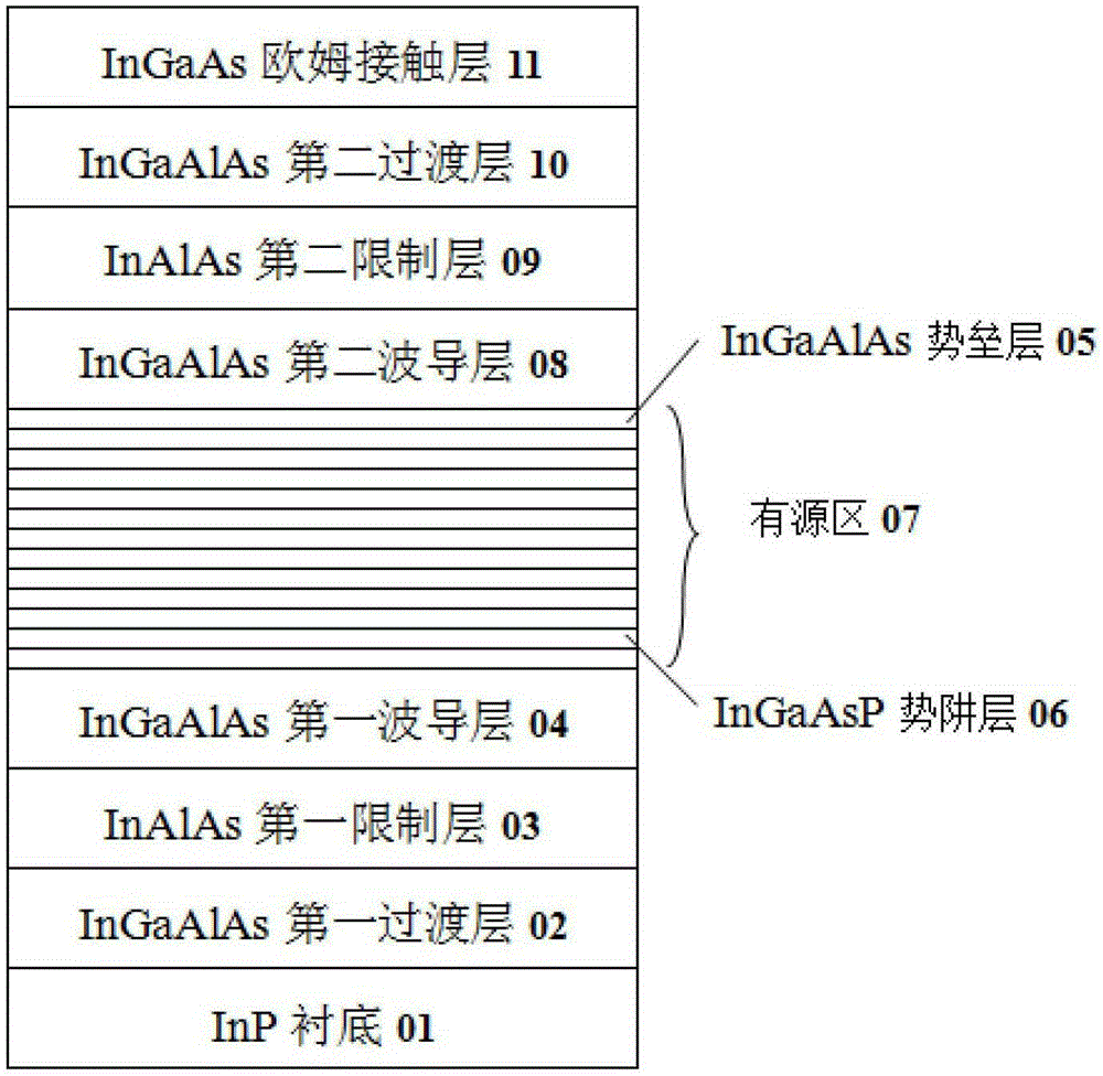
[0039] As mentioned above, in view of the deficiencies in the prior art, the present invention proposes a laser active region and a semiconductor laser including the active region, the semiconductor laser can achieve effective confinement of injected carriers and Uniform distribution of carriers in the active region, lower threshold current and higher differential gain, lower Auger recombination rate and cooling-free operation.

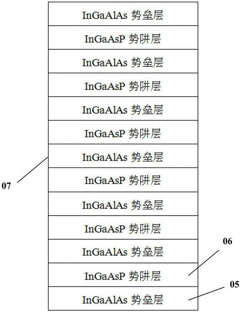
[0040] The laser active region includes a multi-quantum well structure, the material of the potential well layer in the multi-quantum well structure is InGaAsP, the material of the barrier layer in the quantum well structure is InGaAlAs, and the period number of the multi-quantum well structure is is K, the range of K is 3-20, the thickness of the potential well layer is 6-10 nm, and the thickness of the barrier layer is 10-20 nm.

[0041] Spec...


PUM


Abstract

The invention discloses an active area of a laser unit. The active area comprises a multiple-quantum well structure, wherein a potential well layer in the multiple-quantum well structure is made from InGaAsP, and a barrier layer in the multiple-quantum well structure is made from InGaAlAs; a cycle of the multiple-quantum well structure is K, and K ranges from 3 to 20. Furthermore, the invention discloses a semiconductor laser unit and a manufacturing method of the laser unit, wherein the semiconductor laser unit comprises the active area. The semiconductor laser unit provided by the invention has a lower threshold current and higher characteristic temperature, to realize no-refrigeration work; the laser unit has relatively high differential gain, and can provide a laser output in a Tencent Messenger (TM) mode; the laser unit has a relatively high conduction band order, so as to simultaneously restrict injected carriers effectively and distribute the carriers among wells uniformly and enhance the modulation characteristic of the laser unit.

Description

technical field [0001] The invention relates to the field of semiconductor optoelectronics, in particular to an active region of a laser, a semiconductor laser including the active region and a manufacturing method thereof. Background technique [0002] In the field of high-speed optical fiber communication, 1310nm InGaAsP / InP strained quantum well lasers have been extensively and deeply studied. Theory predicts that compared with lattice matching and compressive strain quantum wells, the transverse magnetic field (TM) mode gain provided by the tensile strain quantum well exceeds the transverse electric field (TE) mode gain provided by the compressive strain quantum well, and the tensile strain quantum well can obtain more Optimal device performance, such as lower threshold current, higher differential gain and smaller Auger recombination rate, etc. [0003] At present, the commercialized 1310nm semiconductor laser is mainly based on the InGaAsP / InP material system. However...

Claims


Application Information

Patent Timeline
Patent Type & Authority Patents(China)
IPC IPC(8): H01S5/343
Inventor 曾徐路董建荣李奎龙孙玉润于淑珍赵勇明赵春雨
Owner 苏州市吴中中科育成科技发展有限公司
Why Eureka
Try Eureka