Liquid crystal display panel and device

A technology for liquid crystal display panels and display areas, applied in grounding circuits, instruments, optics, etc., can solve the problem of starting white lines of liquid crystal display panels, and achieve the effect of solving the problem of starting white lines

Active Publication Date: 2012-09-19
BOE TECH GRP CO LTD +1
View PDF6 Cites 12 Cited by
  • Summary
  • Abstract
  • Description
  • Claims
  • Application Information

AI Technical Summary

Problems solved by technology

[0008] The technical problems to be solved by the present invention include fundamentally solving the problem of starting white l

Method used


Image

  • Liquid crystal display panel and device
  • Liquid crystal display panel and device
  • Liquid crystal display panel and device

Examples


Embodiment 1

[0038] This embodiment provides a liquid crystal display panel, which has a display area and an access area, and includes an array substrate and a color filter substrate oppositely arranged, and the array substrate is provided with a thin film defined by gate lines and source lines in the display area. The transistor array is provided with gate leads connected to the gate lines in the access area; the liquid crystal display panel also includes:

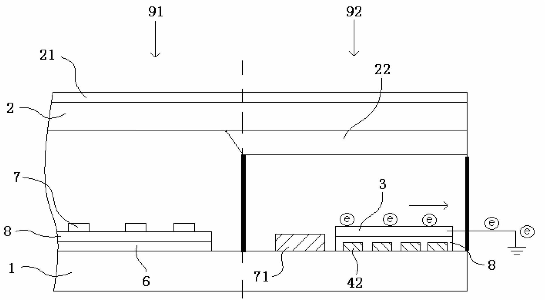
[0039] A grounded, conductive shielding layer located in the access area and used for shielding the induced electromagnetic field caused by the voltage change of the gate lead.

[0040] In the liquid crystal display panel of this embodiment, a grounded conductive shielding layer is provided in the access area, so the induced charge generated by the induced electromagnetic field will be generated in the shielding layer and be quickly led away, so it will not spread to the display area In the middle, there will be no phenomenon of start...

Embodiment 2

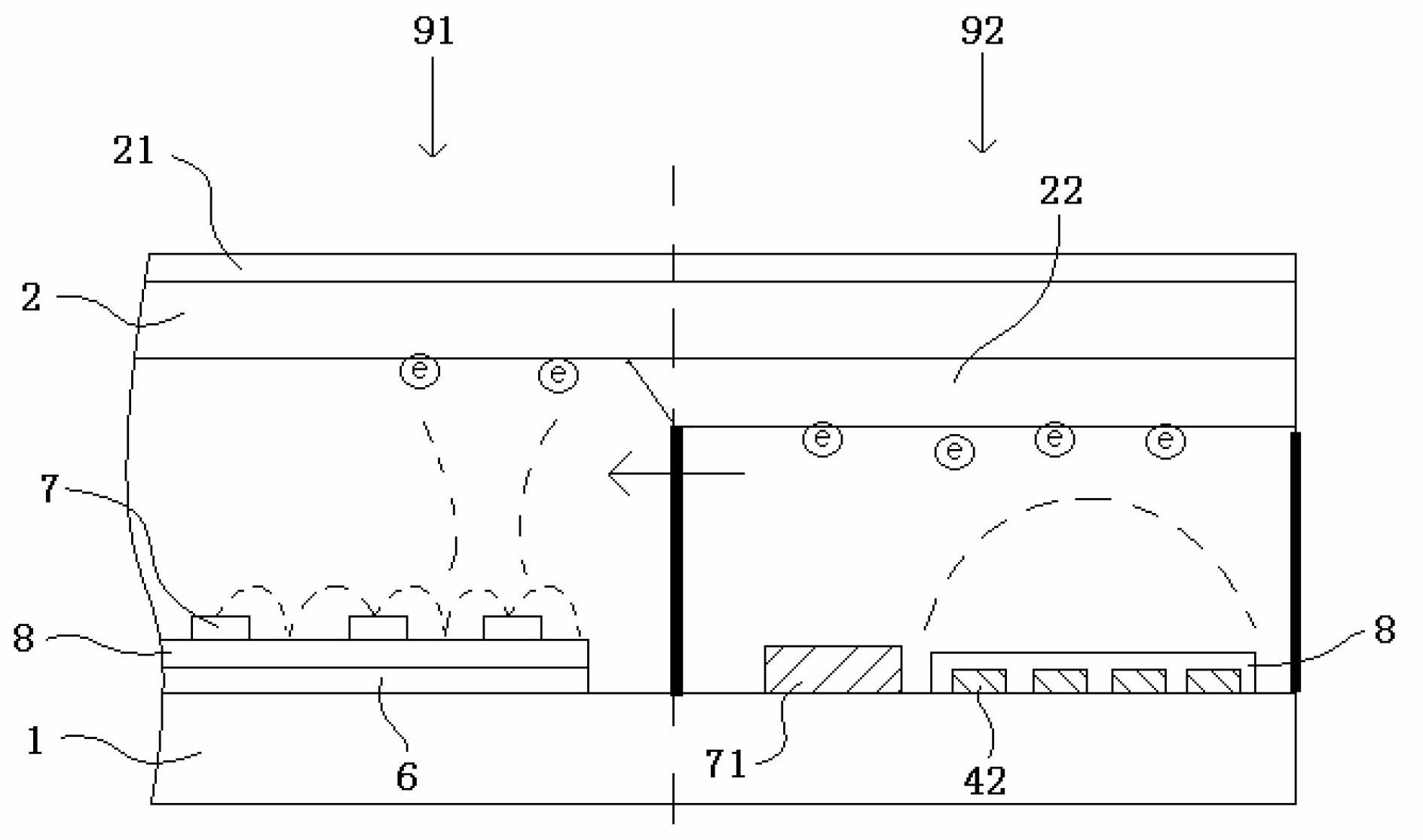
[0042] This embodiment provides a liquid crystal display panel, such as Figure 2 to Figure 5 As shown, it has a display area 91 for displaying, and an access area 92 located outside at least one side of the display area 91 (in this embodiment, there are access areas 92 outside the two opposite sides of the display area 91 as example).

[0043]The liquid crystal display panel includes an array substrate 1 and a color filter substrate 2 oppositely arranged, and liquid crystal material is filled between the array substrate 1 and the color filter substrate 2 .

[0044] Wherein, a plurality of mutually perpendicular gate lines 41 and source lines (not shown in the figure) are provided in the access area 92 of the array substrate 1, and each intersection of the gate lines 41 and source lines defines a thin film transistor array. (not shown in the figure). Wherein, the gate line 41 is connected to the gate of the thin film transistor, the source line is connected to the source of ...

Embodiment 3

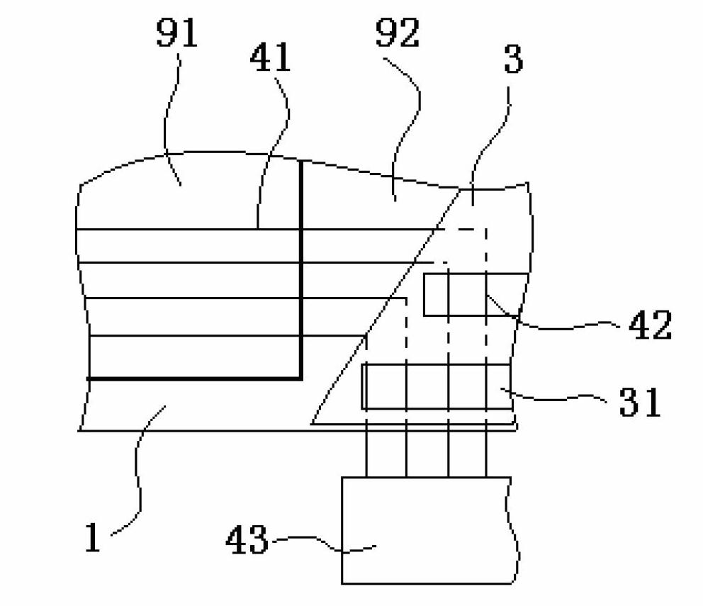
[0057] This embodiment provides a liquid crystal display panel, which has a structure similar to that of the liquid crystal display panel in embodiment 2. The difference between it and the liquid crystal display panel in embodiment 2 is that: Figure 6 , Figure 7 As shown, in the liquid crystal display panel of this embodiment, the shielding layer 3 is not provided on the array plate 1 , but is provided on the color filter substrate 2 (of course still located in the display area 91 ).

[0058] Such as Figure 7 As shown, since the distance between the shielding layer 3 arranged on the color filter substrate 2 and each lead (such as the gate lead 42) on the array plate 1 is relatively large (that is, the value of d is relatively large), the parasitic capacitance itself is relatively large. Therefore, the opening 31 does not need to be provided on the shielding layer 3 at this time, and the width does not need to be changed. Of course, it is also feasible to use structures su...


PUM


Abstract

The invention provides a liquid crystal display panel and device, which belongs to the technical field of liquid crystal display and can solve the problem that the traditional liquid crystal display panel has a starting white line. The liquid crystal display panel disclosed by the invention is provided with a display zone and an access zone and comprises an array base plate and a colorful base plate which are arranged oppositely, wherein the array base plate is provided with a film transistor array limited by a gate electrode line and a source electrode line in the display zone; and the access zone is provided with a gate electrode lead connected with the gate electrode line. The liquid crystal display panel also comprises a shielding layer which is positioned in the access zone, is earthed, conducted and is used for shielding a sensing electromagnetic field caused by the voltage variation of the gate electrode lead. The liquid crystal display device comprises the liquid crystal display panel. The liquid crystal display and device can be used for a horizontal electric field liquid crystal display panel, such as a high-gradient switching-type liquid crystal display panel and a fringing field switching-type liquid crystal display panel.

Description

technical field [0001] The invention belongs to the technical field of liquid crystal display, and in particular relates to a liquid crystal display panel and a device. Background technique [0002] The liquid crystal display panel includes an array substrate and a color filter substrate oppositely arranged, and a liquid crystal material is filled between them. The liquid crystal display panel includes a display area (Active area) for displaying and an access area located outside at least one side of the display area. The display inner area of ​​the array substrate is provided with a plurality of gate lines and source lines perpendicular to each other, and each intersection of the gate lines and source lines forms a thin film transistor array for driving pixel units for display. The access area of ​​the array substrate is provided with a gate lead and a source lead for respectively connecting the gate line and the source line to the gate drive unit and the source drive unit...

Claims


Application Information

Patent Timeline
IPC IPC(8): G02F1/1335G02F1/1362G02F1/1368G02F1/1343
CPCG02F1/13452G02F1/136286G02F1/1333G02F1/1362G02F1/136204G02F2001/136218H05K9/0064G02F1/136218
Inventor 贺伟李兴华朴承翊
Owner BOE TECH GRP CO LTD
Why Eureka
Try Eureka