Check patentability & draft patents in minutes with Patsnap Eureka AI!

Semiconductor memory

一种半导体、存储器的技术,应用在动态随机存取存储器领域,能够解决列地址总线数量大等问题

Active Publication Date: 2012-09-19
SOITEC SA
View PDF3 Cites 5 Cited by
  • Summary
  • Abstract
  • Description
  • Claims
  • Application Information

AI Technical Summary

Problems solved by technology

therefore figure 2 The structure also has the disadvantage of a large number of column address buses

Method used


Image

  • Semiconductor memory
  • Semiconductor memory
  • Semiconductor memory

Examples


Embodiment Construction

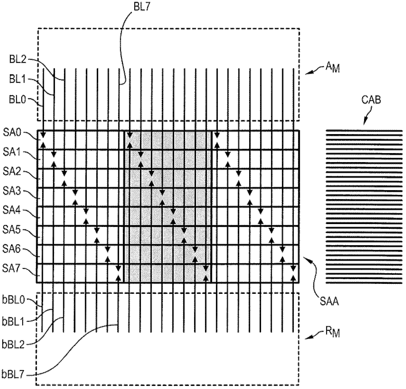
[0035] refer to image 3 , the present invention proposes a semiconductor memory, especially a DRAM, which includes a plurality of bit lines BL0, bBL0, BL1, bBL1, BL2, bBL2, . . . , BL7, bBL7 and a plurality of word lines WL crossing each other. The memory further comprises a memory cell array MCA consisting of a plurality of memory cells arranged in rows and columns at intersections of said bit lines and said word lines. The memory further comprises at least one pair of sense amplifier banks SAB0, ​​SAB1, wherein the pair of sense amplifier banks are arranged on opposite sides of the memory cell array MCA. Each sense amplifier group in a pair comprises a plurality of sense amplifiers SA0, SA2, SA4, SA6; SA1, SA3, SA5, SA7 interleaved in the longitudinal direction of the bit line. The paired sets of sense amplifiers are arranged on opposite sides of the memory cell array MCA.

[0036] image 3A pair of sense amplifier banks SAB0, ​​SAB1 is described, where each bank has fou...


PUM


Abstract

The invention relates to a semiconductor memory, comprising: - bit lines, - a memory cell array and, - at least one pair of sense amplifier banks, wherein each sense amplifier is connected to a corresponding bit line according to an interleaved arrangement resulting in interconnect spaces available in each sense amplifier bank of the pair parallel to the bit lines, characterized in that each sense amplifier bank further comprises at least one local column decoder for selecting at least one sense amplifier of the sense amplifier bank, the local column decoder being coupled to the at least one sense amplifier of the sense amplifier bank by means of an output line running in an available interconnect space parallel to the bit lines.

Description

technical field [0001] The present invention relates generally to semiconductor memories, and more particularly to dynamic random access memories (DRAMs) in which local column decoders are associated with interleaved sense amplifiers. Background technique [0002] Basically, DRAM is an integrated circuit that stores data in binary form (such as "1" or "0") in a large number of cells. The data is stored in the cell as a charge on a capacitor located in the cell. Typically, a high logic level is approximately equal to the supply voltage and a low logic level is approximately equal to ground. [0003] The cells of conventional DRAM are arranged in an array so that individual cells can be addressed and accessed. The array can be thought of as rows and columns of cells. Each row includes word lines interconnecting the cells on that row with common control signals. Similarly, each column includes bit lines coupled to at most one cell in each row. Thus, word lines and bit line...

Claims


Application Information

Patent Timeline
Patent Type & Authority Applications(China)
IPC IPC(8): G11C7/18G11C7/06
CPCG11C11/4091G11C7/065G11C11/4097G11C11/4096
Inventor R·费兰特G·恩德斯C·马聚尔
Owner SOITEC SA
Features
  • R&D
  • Intellectual Property
  • Life Sciences
  • Materials
  • Tech Scout
  • Unparalleled Data Quality
  • Higher Quality Content
  • 60% Fewer Hallucinations
Learn More