
Light-emitting diode device and method for manufacturing the same

A technology of light-emitting diodes and manufacturing methods, which is applied in the direction of electrical components, electrical solid-state devices, semiconductor devices, etc., can solve the problem of uneven current distribution of large chip sizes, avoid the effect of sudden drop in efficiency, improve the quality of epitaxy, and reduce production costs. Effect

Inactive Publication Date: 2012-09-19
CHI MEI LIGHTING TECH +1
View PDF5 Cites 9 Cited by
  • Summary
  • Abstract
  • Description
  • Claims
  • Application Information

AI Technical Summary

Problems solved by technology

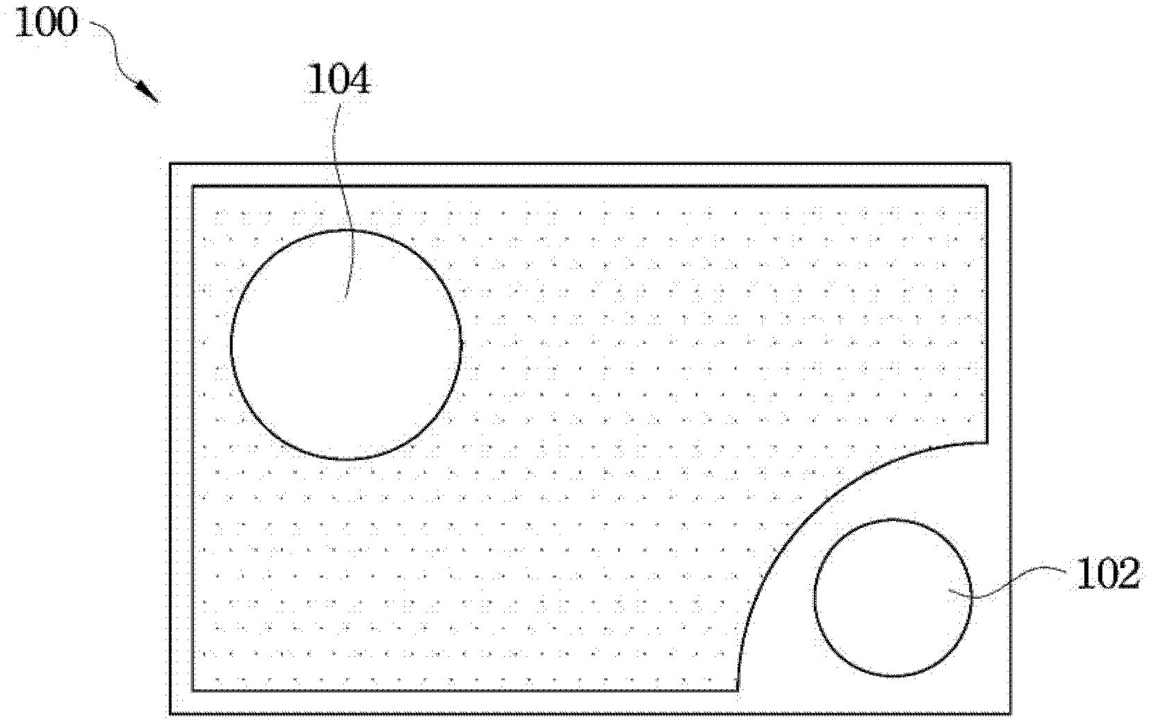
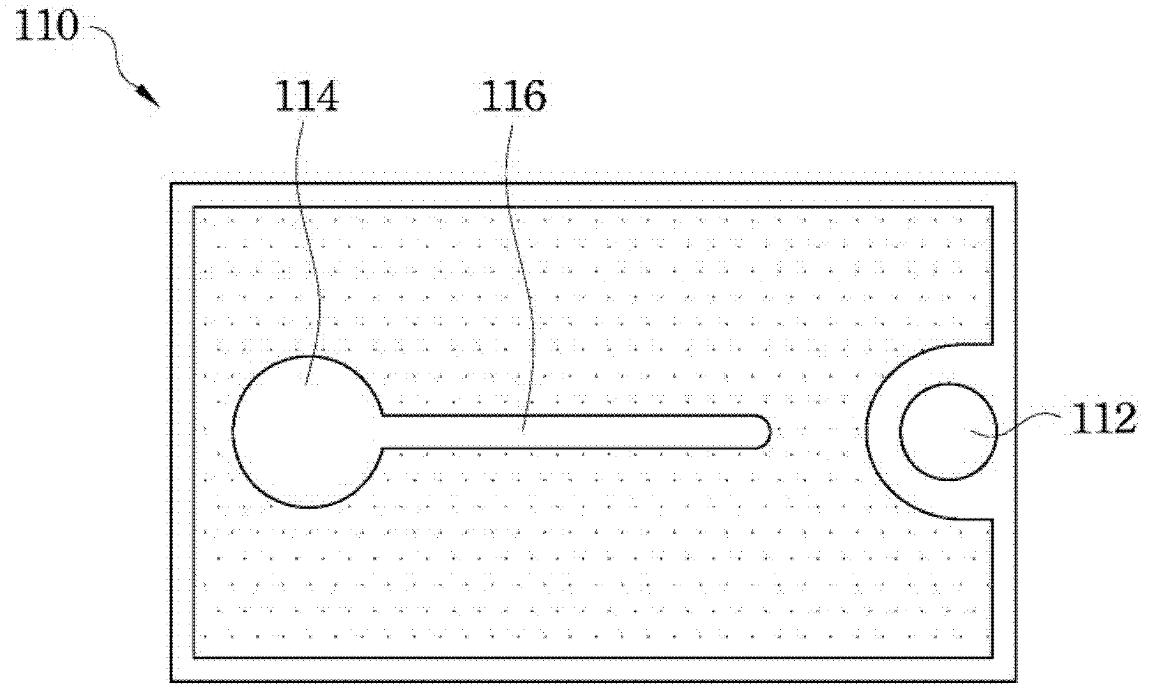
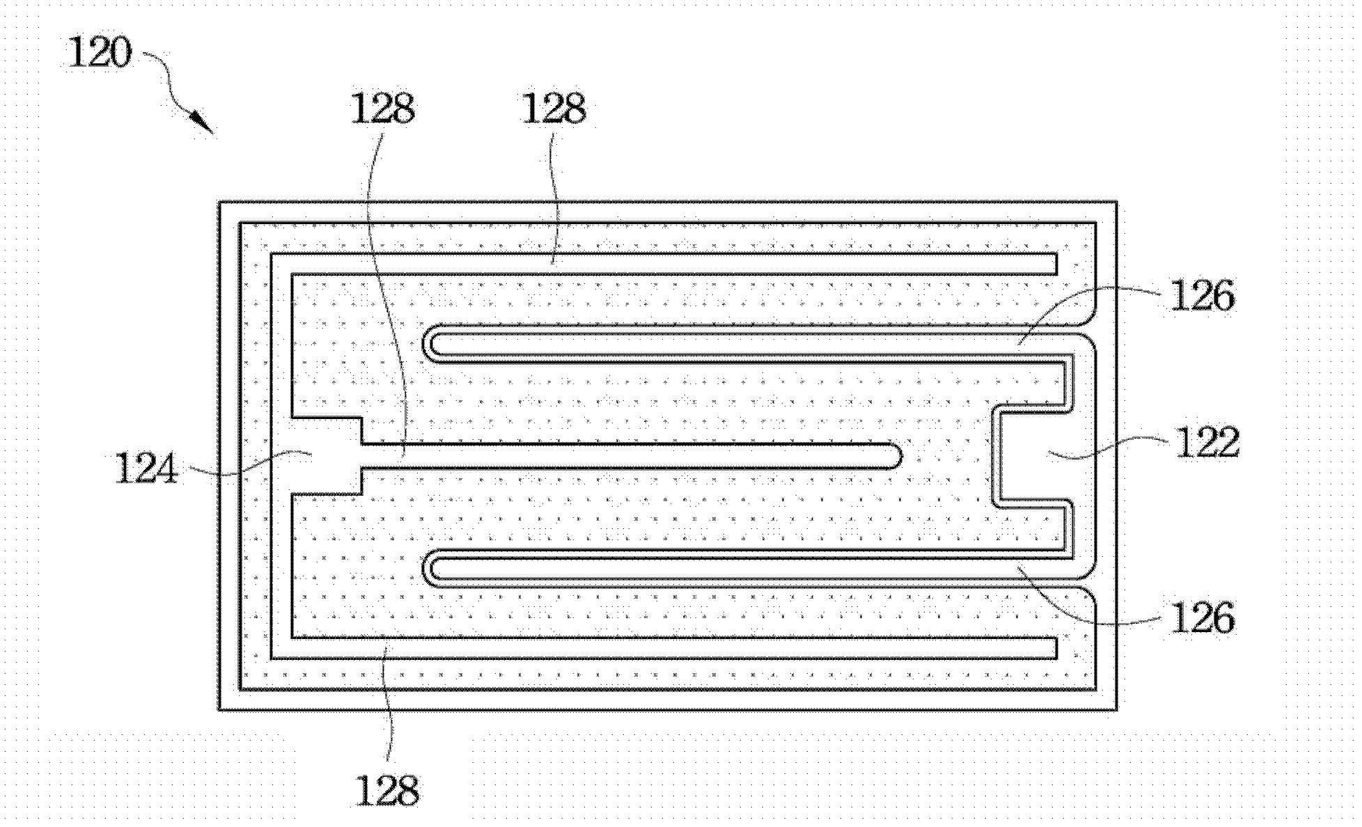
[0010] Therefore, the object of the present invention is to provide a light-emitting diode element and its manufacturing method, which includes several small light-emitting structures connected in series, so it can solve the problem of uneven current distribution of large chip size, and can be driven by a small current , to avoid the effect of sudden drop in efficiency caused by high current drive

Method used


Image

  • Light-emitting diode device and method for manufacturing the same
  • Light-emitting diode device and method for manufacturing the same
  • Light-emitting diode device and method for manufacturing the same

Examples


Embodiment Construction

[0063] Please refer to Figure 3F , which is a cross-sectional view illustrating a light emitting diode element according to an embodiment of the present invention. In this embodiment, the light emitting diode element 238 mainly includes the current blocking structure formed by the substrate 200, the undoped semiconductor layer 204, the lightly doped semiconductor layer 206 and the current blocking layer 208, and is separately arranged on the current blocking layer. There are several light emitting structures 230a, 230b and 230c on the structure. Wherein, an insulating spacer 234 is provided between any adjacent two of the light emitting structures 230a, 230b, and 230c, so as to electrically isolate the adjacent light emitting structures 230a, 230b, and 230c. The light emitting diode element 238 further includes a plurality of wires 236 to electrically connect the light emitting structures 230 a , 230 b and 230 c in series. Therefore, the light-emitting diode element 238 is ...


PUM


Abstract

The invention discloses a light-emitting diode device and a method for manufacturing the same. An undoped semiconductor layer and a current blocking structure of the light-emitting diode device are disposed on a substrate in sequence. Light-emitting structures of the light-emitting diode device are separately disposed on the current blocking structure. Each of the light-emitting structures has a first conductivity type semiconductor layer, an active layer and a second conductivity type semiconductor layer arranged on the first conductivity type semiconductor layer in sequence, and a first electrode and a second electrode, respectively located on the other part of the first conductivity type semiconductor layer and the second conductivity type semiconductor layer. The first conductivity type semiconductor layer and the second conductivity type semiconductor layer have different conductivity types. Insulating spacers of the light-emitting diode device are respectively located between the adjacent light-emitting structures. Conductive wires of the light-emitting diode device respectively connect the first electrode of one of the adjacent light-emitting structures and the second electrode of the other light-emitting structure in sequence.

Description

technical field [0001] The present invention relates to a light emitting element, and in particular to a light emitting diode (LED) element and a manufacturing method thereof. Background technique [0002] With the vigorous development of light-emitting diode technology, and the application of light-emitting diodes in light sources has the advantages of thinning, power saving and mercury-free, so the technology of light-emitting diodes has a tendency to gradually replace traditional light-emitting technologies. [0003] As the proportion of light-emitting diodes in applications of high-brightness products such as lighting and automotive headlights gradually increases, the requirements for the brightness of light-emitting diode chips are also increasing. In order to obtain higher brightness, it is necessary to use a larger current for driving in operation, so as to increase the brightness of the light-emitting diode chip. [0004] However, the increase of the current may cau...

Claims


Application Information

Patent Timeline
Patent Type & Authority Applications(China)
IPC IPC(8): H01L33/14H01L33/02H01L33/42H01L33/32H01L33/00H01L33/62H01L25/075
CPCH01L33/145H01L33/62H01L27/156H01L2924/0002H01L2924/00
Inventor 汪信全吴浩青
Owner CHI MEI LIGHTING TECH
Learn More