Bi-module masing semiconductor laser capable of achieving mode distance of 100GHz

A laser and semiconductor technology, applied in semiconductor lasers, lasers, laser parts and other directions, can solve the problems of complex structure, difficult research, difficult to integrate, etc., and achieve the effect of compact device structure and simple manufacturing process

Active Publication Date: 2012-09-19
INST OF SEMICONDUCTORS - CHINESE ACAD OF SCI
View PDF4 Cites 6 Cited by
  • Summary
  • Abstract
  • Description
  • Claims
  • Application Information

AI Technical Summary

Problems solved by technology

However, for 100Gbit/s optical signal clock recovery, there are relatively few related research reports. For fiber mode-locked lasers, it can theoretically work in a 100Gbit/s system. However, this solution is not easy to inte

Method used


Image

  • Bi-module masing semiconductor laser capable of achieving mode distance of 100GHz
  • Bi-module masing semiconductor laser capable of achieving mode distance of 100GHz
  • Bi-module masing semiconductor laser capable of achieving mode distance of 100GHz

Examples


Embodiment Construction

[0023] In order to make the object, technical solution and advantages of the present invention clearer, the present invention will be described in further detail below in conjunction with specific embodiments and with reference to the accompanying drawings.

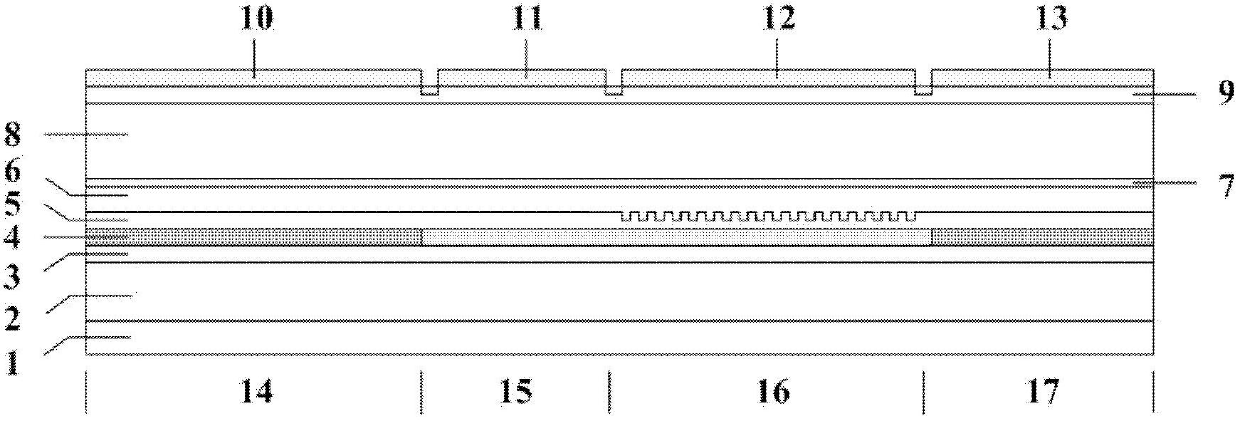
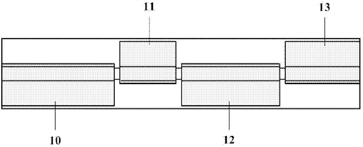
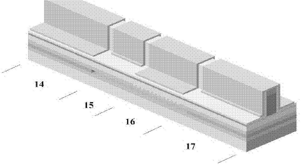
[0024] see figure 1 , 2 . In the embodiment shown in 3, the dual-mode lasing semiconductor laser that can achieve a mode spacing of 100 GHz provided by the embodiment of the present invention includes:

[0025] A substrate 1, which is an n-type InP substrate;

[0026] An n-InP buffer layer 2, which is fabricated on the substrate 1;

[0027] An InGaAsP lower confinement layer 3, the InGaAsP lower confinement layer 3 is fabricated on the n-InP buffer layer 2, its thickness is about 120 nm, and the material bandgap wavelength is 1.3 microns;

[0028] A multi-quantum well active layer 4, the multi-quantum well active layer 4 is made on the InGaAsP lower confinement layer 3, the multi-quantum well active layer 4 is five qua...


PUM

PropertyMeasurementUnit
Lengthaaaaaaaaaa

Abstract

The invention discloses a bi-module masing semiconductor laser capable of achieving a mode distance of 100GHz. The bi-module masing semiconductor laser comprises a substrate, an n-InP buffering layer, an InGaAsP lower limiting layer, a multi-quantum well active layer, an InGaAsP upper limiting layer, a p-InP layer, a p-InGaAsP etching prevention layer, an upper p-InP cover layer, a p-InGaAs ohm contact layer and metal electrode layers, wherein a Bragg grating structure is formed on the surface of the InGaAsP upper limiting layer and is processed in a grating region; an isolating ditch is formed on the p-InGaAs ohm contact layer and divides the p-InGaAs ohm contact layer into four segments; the metal electrode layers are respectively formed on each of the four segments of the p-InGaAs ohm contact layer; and the four segments of the p-InGaAs ohm contact layer are respectively corresponding to the four segment structures of the bi-module masing semiconductor laser, wherein the four segment structures comprise a front gain region, a phase region, a grating region and a back amplification region.

Description

technical field [0001] The invention belongs to the technical field of semiconductor optoelectronics, and is a dual-mode lasing semiconductor laser capable of realizing a mode spacing of 100 GHz. Background technique [0002] With the rapid development of the Internet, the scale of the switching system in the communication network is getting larger and higher, and the operating speed is getting higher and higher. The future large-scale switching system will need to process information with a total amount of hundreds of Tbit / s, which makes the traditional electronic-based Due to the limitation of "electronic bottleneck", the network of signal processing technology is gradually becoming difficult to deal with. Therefore, the all-optical network based on all-optical signal processing technology using all-optical switching and all-optical routing will be the development trend of future networks. . [0003] The process of synchronously extracting an optical clock signal from opt...

Claims


Application Information

Patent Timeline
IPC IPC(8): H01S5/343H01S5/042
Inventor 余力强赵玲娟朱洪亮吉晨陆丹潘教青王圩
Owner INST OF SEMICONDUCTORS - CHINESE ACAD OF SCI
Why Eureka
Try Eureka