Liquid crystal display device and manufacturing method therefor

A technology of a liquid crystal display device and a manufacturing method, which is applied in the direction of instruments, nonlinear optics, optics, etc., can solve problems such as hindering the conduction of terminal circuit chips, and achieve the effect of suppressing expansion and reducing non-display areas

Inactive Publication Date: 2012-09-19
SHARP KK
View PDF7 Cites 13 Cited by
  • Summary
  • Abstract
  • Description
  • Claims
  • Application Information

AI Technical Summary

Problems solved by technology

When the alignment film material reaches the terminal area of ​​the frame area, multiple terminals are covered by the alignment film as an insulating film, and as a result, the conduction between the terminal and the circuit chip mounted on the terminal is hindered.

Method used


Image

  • Liquid crystal display device and manufacturing method therefor
  • Liquid crystal display device and manufacturing method therefor
  • Liquid crystal display device and manufacturing method therefor

Examples


Embodiment approach 1

[0047] Figure 1 to Figure 6 Embodiment 1 of this invention is shown.

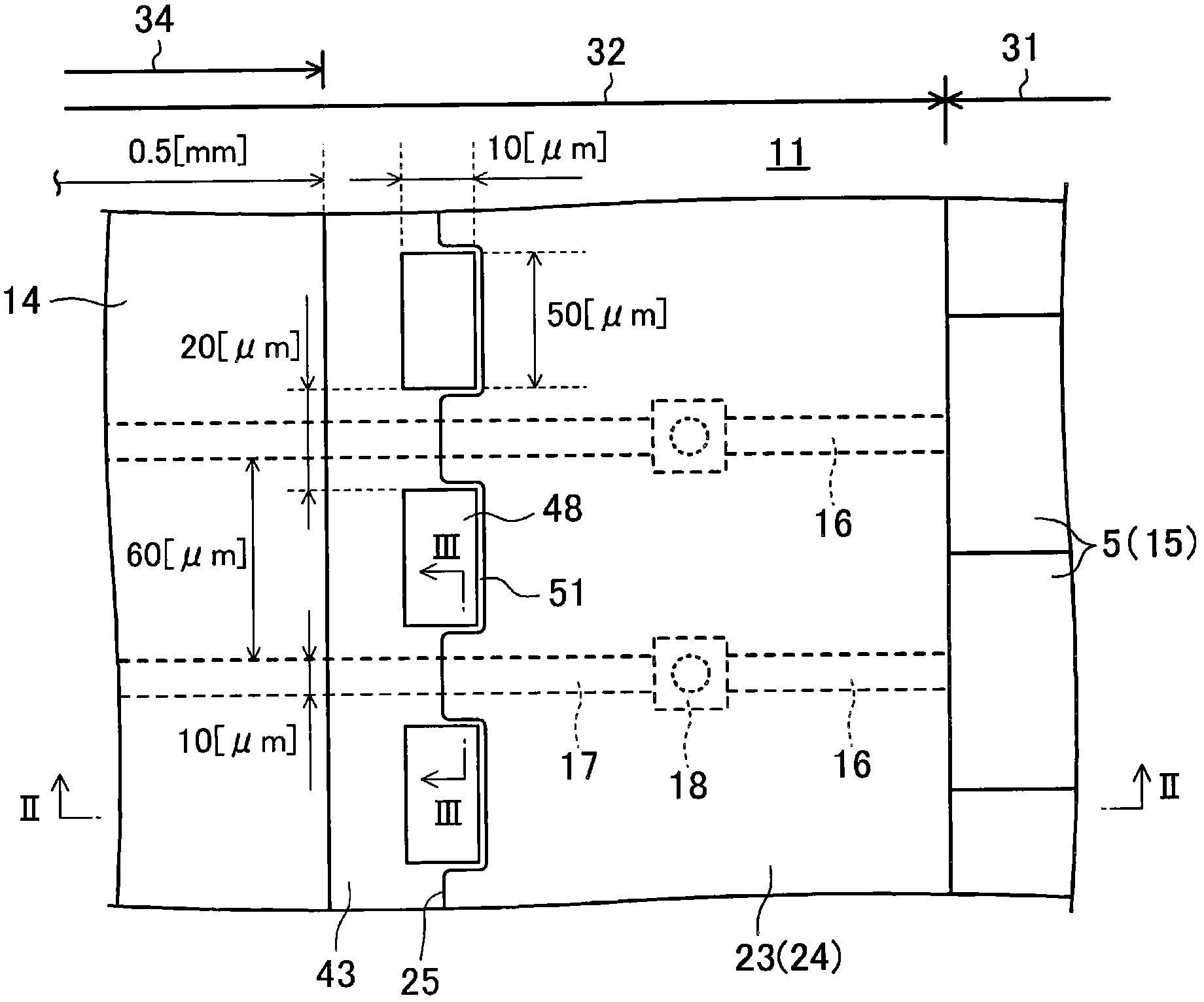
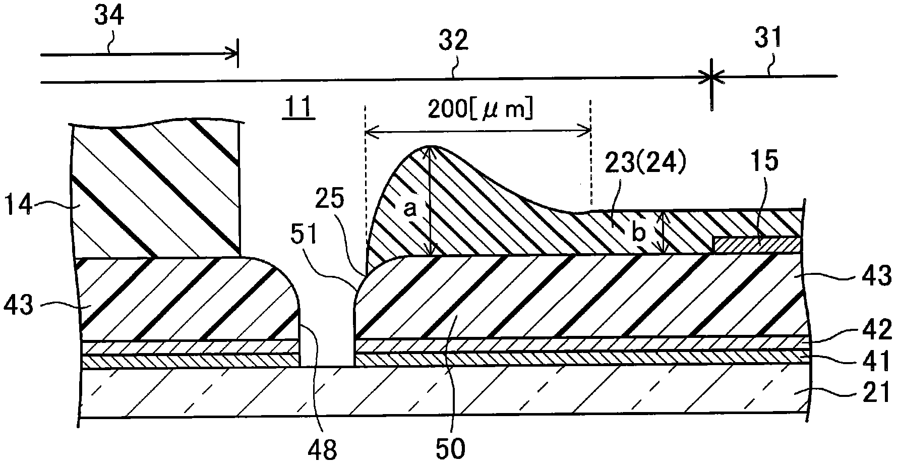
[0048] figure 1 It is a plan view showing an enlarged part of the TFT substrate 11 of the first embodiment. figure 2 yes figure 1 The II-II line sectional view. image 3 yes figure 1 Sectional view of line III-III. Figure 4 It is a plan view showing a schematic configuration of the liquid crystal display device 1 of the first embodiment.

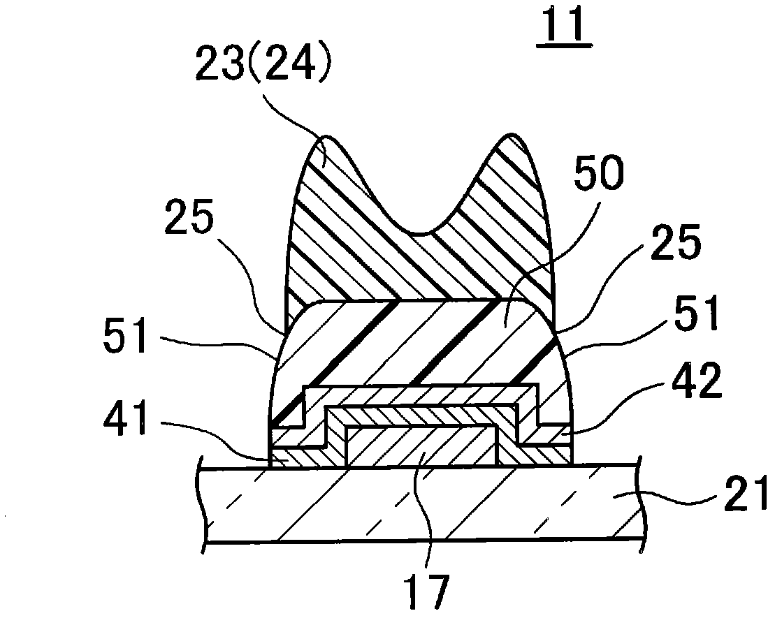
[0049] in addition, Figure 5It is an enlarged plan view showing a part of the counter substrate 12 of the first embodiment. Figure 6 yes Figure 5 The VI-VI line sectional view. Figure 7 With Figure 4 Comparable diagram of line section VII-VII. Figure 8 It is an enlarged cross-sectional view showing the supporting structure portion 50 of the TFT substrate 11 .

[0050] Figure 9 It is an enlarged plan view showing a part of the TFT substrate 11 . In addition, in Figure 9 In , the illustration of the alignment film 23 and the concave portion 48 w...

Embodiment approach 2

[0106] Figure 10 Embodiment 2 of this invention is shown.

[0107] Figure 10 It is an enlarged cross-sectional view illustrating the structure of the TFT substrate 11 according to the second embodiment. In addition, in each of the following embodiments, for the Figure 1 to Figure 8 The same reference numerals are attached to the same parts, and detailed description thereof will be omitted.

[0108] In Embodiment 1 above, the planarizing film 43 is formed on the sealing member forming region 34 , but in Embodiment 2, the sealing member 14 is formed on the glass substrate 21 , and there is no intervening support between the sealing member 14 and the glass substrate 21 . The planarizing film 43 is a constituent material of the structural portion 50 .

[0109] That is, in the sealing member forming region 34 of the TFT substrate 11 , the gate insulating film 41 , the passivation film 42 , and the planarizing film 43 are removed from the glass substrate 21 by etching or the ...

Embodiment approach 3

[0112] Figure 11 Embodiment 3 of this invention is shown.

[0113] Figure 11 It is an enlarged cross-sectional view showing the structure of the TFT substrate of Embodiment 3. FIG.

[0114] In the first embodiment described above, the plurality of recesses 48 are formed at predetermined intervals from the sealing member 14 , but in the third embodiment, the sealing member 14 is also formed inside each recess 48 . That is, the sealing member 14 is arranged in contact with the side end of the support structure portion 50 in a state of being separated from the edge portion 25 of the alignment film 23 (orientation film material 24 ).

[0115]Therefore, according to this third embodiment as well, by providing the above-mentioned support structure portion 50 , the same effect as that of the above-mentioned first embodiment can be obtained. In addition, since the sealing member 14 is in contact with the side end of the support structure portion 50 while being separated from the ...


PUM

PropertyMeasurementUnit
viscosityaaaaaaaaaa
thicknessaaaaaaaaaa
thicknessaaaaaaaaaa

Abstract

An alignment film formed by curing of an alignment film material having fluidity is formed so as to extend from a pixel region toward a frame region on the liquid crystal layer side of each of a first substrate and a second substrate. The first substrate and / or the second substrate comprises a support substrate, and a support structure part which is formed above the support substrate and at least the surface of which on the side opposite to the support substrate is covered directly with the alignment film. The support structure part has a side section which is formed such that a tangent plane inclines to the outside of the support structure part toward the support substrate. The side section of the support structure part is disposed in the frame region and supports an end edge section of the alignment film.

Description

technical field [0001] The present invention relates to a liquid crystal display device and a manufacturing method thereof, in particular to the control of the coating area of ​​an alignment film. Background technique [0002] A liquid crystal display device generally has a structure in which a liquid crystal layer is sealed between a pair of substrates. One of the pair of substrates is a TFT substrate on which a plurality of gate wirings, a plurality of source wirings, a plurality of pixel electrodes, a plurality of TFTs, and the like are formed. The other of the pair of substrates is an opposing substrate on which a common electrode shared by a plurality of pixel electrodes is formed. The liquid crystal layer is surrounded and sealed by a frame-shaped sealing member between the TFT substrate and the counter substrate. [0003] A pixel region serving as a display region and a frame region serving as a non-display region provided around the outside of the pair of substrate...

Claims


Application Information

Patent Timeline
Patent Type & Authority Applications(China)
IPC IPC(8): G02F1/1337G02F1/1333G02F1/1339
CPCG02F1/133788G02F1/1339G02F1/1337G02F2001/133776G02F1/133776
Inventor 森胁弘幸神崎庸辅
Owner SHARP KK
Why Eureka
Try Eureka