Electrophotographic photosensitive member and electrophotographic apparatus
A photosensitive member, electrophotography technology, applied in optics, electrography, instruments, etc., can solve problems such as insufficient adhesion, achieve the effects of excellent photosensitive characteristics and charging characteristics, degradation suppression, and sufficient image forming ability
- Summary
- Abstract
- Description
- Claims
- Application Information
AI Technical Summary
Problems solved by technology
Method used
Image
Examples
Embodiment 1
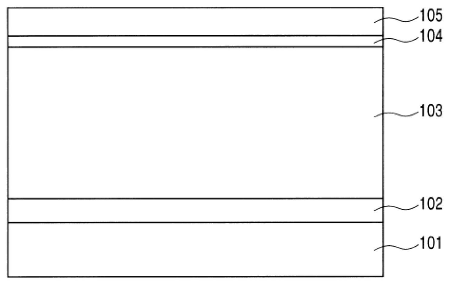
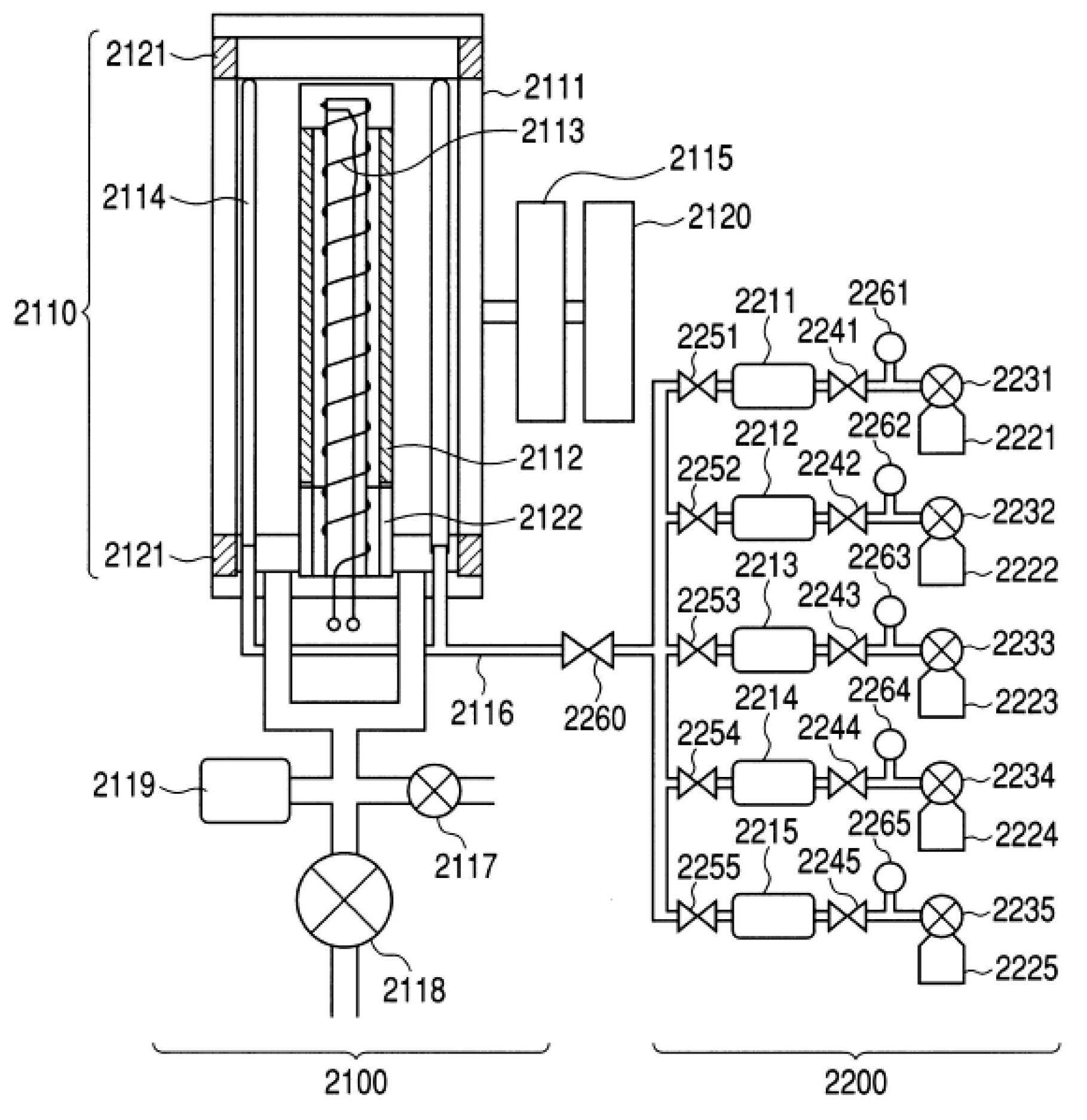
[0099] On a cylindrical substrate (an aluminum cylindrical substrate having a diameter of 80mm, a length of 358mm and a thickness of 3mm, and mirror-polished), by using figure 2 An electrophotographic photosensitive member to be negatively charged was produced under the following conditions shown in Table 1 using the plasma processing apparatus shown and a high-frequency power source using an RF band as a frequency. At this time, a lower charge injection preventing layer, a photoconductive layer, an upper charge injection preventing layer, and a surface layer are formed in this order (layer formation). In addition, when forming the surface layer, set high-frequency power, SiH 4 Flow rate and CH 4 flow rate. In addition, for each film-forming condition, an electrophotographic photosensitive member to be negatively charged was produced.
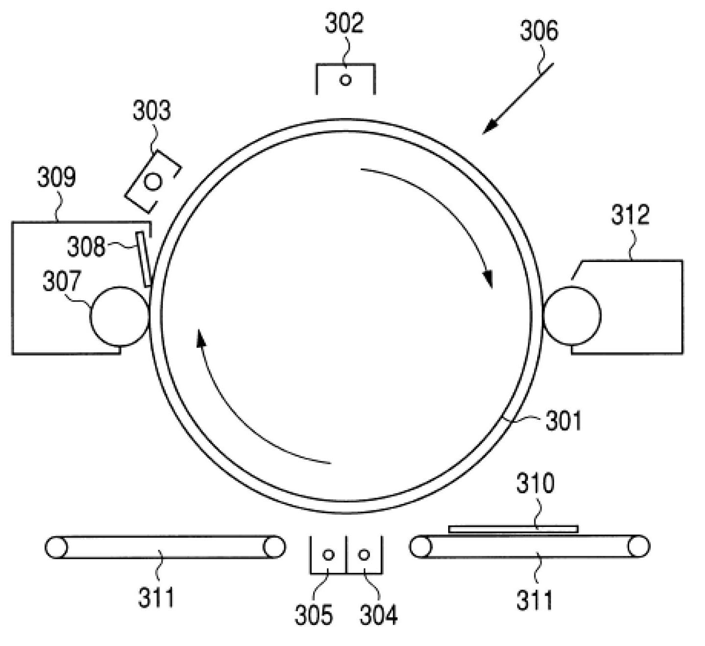
[0100]The produced electrophotographic photosensitive member to be negatively charged was installed in an electrophotographic apparatus ha...
Embodiment 2
[0184] Two electrophotographic photosensitive members to be negatively charged were produced in the same manner as in Example 1 except that the surface layers were produced under the conditions shown in Table 7 below.
[0185] The produced electrophotographic photosensitive member to be negatively charged was evaluated in a similar manner to Example 1.
[0186] These results are shown in Tables 9 and 10. In addition, the boron atom content was 300 atomic ppm±10 atomic ppm relative to the silicon atom content in the upper charge injection preventing layer, and C / (Si+C) in the upper charge injection preventing layer was 0.30±0.01.
[0187] Table 7
[0188] Film forming condition No.
Embodiment 3
[0202] Two electrophotographic photosensitive members to be negatively charged were produced in the same manner as in Example 1 except that the surface layers were produced under the conditions shown in Table 11 below.
[0203] The produced electrophotographic photosensitive member to be negatively charged was evaluated in a similar manner to Example 1.
[0204] These results are shown in Tables 12 and 13 together with the results of film formation condition No. 10 in Example 2. In addition, the boron atom content was 300 atomic ppm±10 atomic ppm relative to the silicon atom content in the upper charge injection preventing layer, and C / (Si+C) in the upper charge injection preventing layer was 0.30±0.01.
[0205] Table 11
[0206] Film forming condition No.
17
18
19
20
21
22
23
24
25
SiH 4 [mL / min(standard)]
26
26
32
26
26
26
26
26
26
CH 4 [mL / ...
PUM
 Abstract
Description
Claims
Application Information


