
Display panel and inspection method thereof

A technology for a display panel and an inspection method, which is applied to static indicators, instruments, electroluminescent light sources, etc., can solve the problem that the source driver 94 has not been installed yet.

Inactive Publication Date: 2012-09-19
SHARP KK
View PDF5 Cites 16 Cited by
  • Summary
  • Abstract
  • Description
  • Claims
  • Application Information

AI Technical Summary

Problems solved by technology

In addition, at the time of panel inspection, the source driver 94 has not yet been mounted on the glass substrate.

Method used


Image

  • Display panel and inspection method thereof
  • Display panel and inspection method thereof
  • Display panel and inspection method thereof

Examples


no. 1 approach

[0101] (1.1 overall structure)

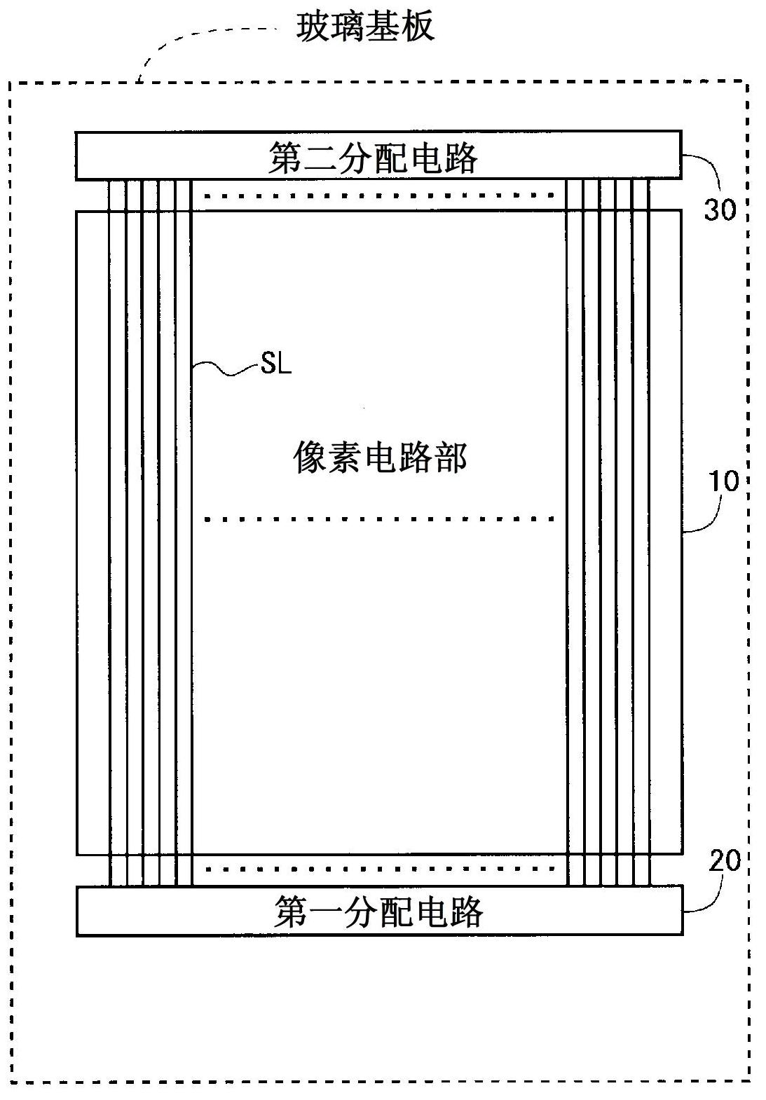
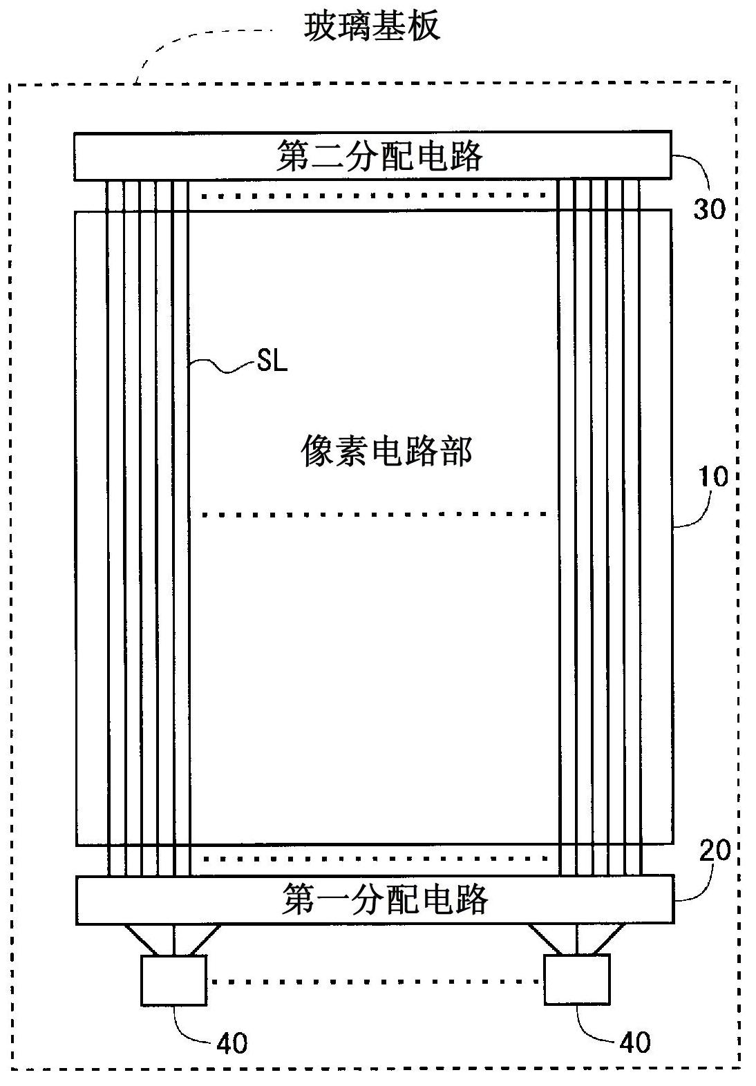
[0102] figure 2 It is a block diagram showing the configuration of main parts of the liquid crystal panel according to the first embodiment of the present invention. Such as figure 2 As shown, this liquid crystal panel includes: a pixel circuit unit 10 serving as an area for displaying an image; and a first distribution circuit 20 and a second distribution circuit 30 having a function of switching and outputting a signal supplied from the outside to a plurality of signal lines. The pixel circuit unit 10, the first distribution circuit 20, and the second distribution circuit 30 are formed on one of the two glass substrates constituting the liquid crystal panel (generally referred to as an "array substrate").

[0103] The pixel circuit section 10 includes a plurality of source bus lines (video signal lines) SL, a plurality of gate bus lines (scanning signal lines), and a plurality of pixels respectively provided corresponding to the intersect...

no. 2 approach

[0159] (2.1 Structure and operation of distribution circuit)

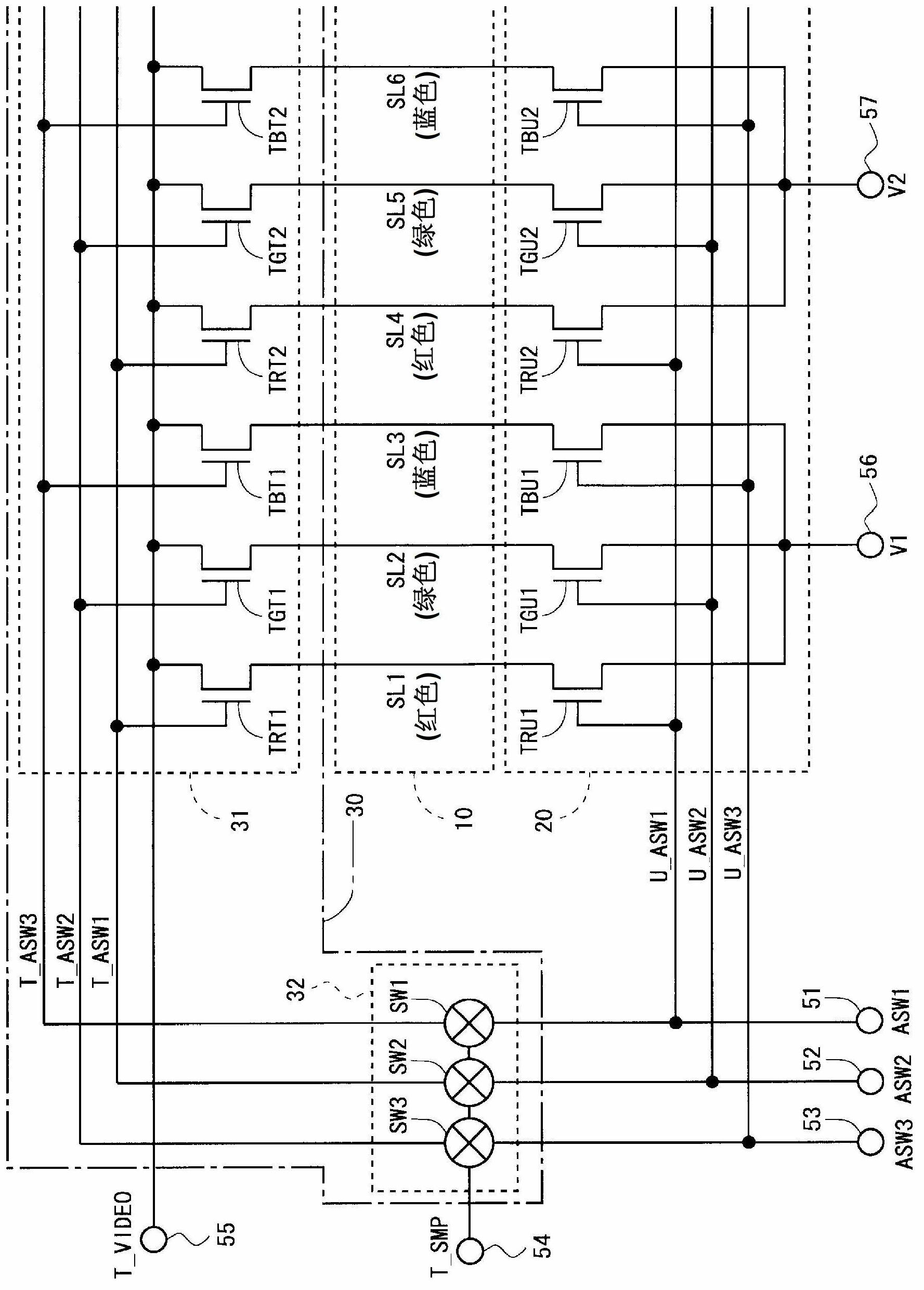
[0160] Figure 19 It is a circuit diagram showing the detailed configuration of the first distribution circuit 20 and the second distribution circuit 30 according to the second embodiment of the present invention. In addition, in figure 1 In , only six source bus lines SL1 to SL6 among the plurality of source bus lines are shown. Regarding the overall structure of the liquid crystal panel, since it is the same as that of the above-mentioned first embodiment, description thereof will be omitted (see figure 2 , image 3 ). In this embodiment, unlike the above-mentioned first embodiment, a demultiplexer having one input and six outputs is provided in the first distribution circuit 20 for every six source bus lines. Similarly, the distribution unit 35 in the second distribution circuit 30 is also provided with a demultiplexer with 1 input and 6 outputs for every six source bus lines. when looking at the Figur...

no. 3 approach

[0190] (3.1 Structure)

[0191] The structure of the liquid crystal panel of the third embodiment of the present invention is the same as that of the first embodiment (refer to Figure 1 to Figure 5 ). In the first embodiment, the second distribution circuit 30 is used as a circuit for panel inspection (typically before mounting the driver IC), but in this embodiment, it is used as a circuit for precharging (pre-charging) the source bus line. circuit use. Therefore, this second distribution circuit 30 can be used not only as a circuit for panel inspection, but also as a circuit for precharging. In addition, for convenience of description, the "video signal for testing" in the first embodiment is called "video signal for precharging", and the "switch for inspection" in the first embodiment is called "switch for precharging".

[0192] (3.2 Driving method)

[0193] Below, refer to Figure 29 , the driving method of the source bus line when the second distribution circuit 30 ...


PUM


Abstract

Provided is a display panel in which failures in sampling switches, which operate at normal times, can also be detected during inspections of the panel, without increasing the circuit size. The display panel includes: a single-input three-output demultiplexer that is provided on one side of the source bus lines and that includes sampling switches for sampling video signals; and a single-input three-output demultiplexer that is provided on the other side of the source bus lines, that includes inspection switches provided in correspondence with the respective sampling switches, and that employs test video signals (T_VIDEO) as the input signals. If one of the three control signals (ASW1 to ASW3) which control the state of the sampling switches and the state of the inspection switches is defined as the target control signal, the source bus line connected to the sampling switch that is turned on by the target control signal is different from the source bus line connected to the inspection switch that is turned on by the target control signal.

Description

technical field [0001] The present invention relates to a display panel, and more specifically, to a display panel including a demultiplexer for distributing a video signal to a plurality of video signal lines, and an inspection method thereof. Background technique [0002] Conventionally, a liquid crystal module is produced by mounting a driver IC (integrated circuit for driving) on ​​a liquid crystal panel in a module manufacturing process after passing through an array manufacturing process and a panel manufacturing process. Generally, before mounting a driver IC, an inspection (hereinafter, referred to as "panel inspection") is performed to investigate whether or not there is a defect in a liquid crystal panel. Therefore, an inspection circuit may be formed in advance on a substrate constituting a liquid crystal panel. Figure 31 It is a block diagram showing a configuration of a main part of a liquid crystal module in which a driver IC is mounted on a liquid crystal pan...

Claims


Application Information

Patent Timeline
Patent Type & Authority Applications(China)
IPC IPC(8): G09G3/20G02F1/133G09G3/30G09G3/36H01L51/50H05B33/12
CPCG09G3/3688G09G3/006G09G2310/0297G09G3/3611G09G2330/12
Inventor 高桥功古田成村上祐一郎佐佐木宁
Owner SHARP KK
Learn More