Supercharge Your Innovation With Domain-Expert AI Agents!

Liquid crystal display device, array substrate thereof and manufacturing method

A technology of liquid crystal display devices and array substrates, applied in the manufacture of array substrates and array substrates, and in the field of liquid crystal display devices, can solve the problems of waste, slow response rate of liquid crystal molecules, and failure of normal deflection and alignment of liquid crystal molecules, etc., to reduce the cost of defective products Effect

Active Publication Date: 2012-09-26
CHANGSHA HKC OPTOELECTRONICS CO LTD
View PDF4 Cites 13 Cited by
  • Summary
  • Abstract
  • Description
  • Claims
  • Application Information

AI Technical Summary

Problems solved by technology

[0004] However, if the voltage circuit is abnormal during this process, and the electric field cannot be generated between the color filter substrate and the array substrate, the liquid crystal molecules cannot be normally deflected and aligned, resulting in poor display or slow response rate of liquid crystal molecules in the produced liquid crystal display device. status
In addition, the PSVA process is an irreversible process, and there is no way to repair the LCD device in the subsequent process, resulting in serious waste

Method used


Image

  • Liquid crystal display device, array substrate thereof and manufacturing method
  • Liquid crystal display device, array substrate thereof and manufacturing method
  • Liquid crystal display device, array substrate thereof and manufacturing method

Examples


Embodiment Construction

[0023] The present invention will be described in detail below in conjunction with the embodiments and the accompanying drawings.

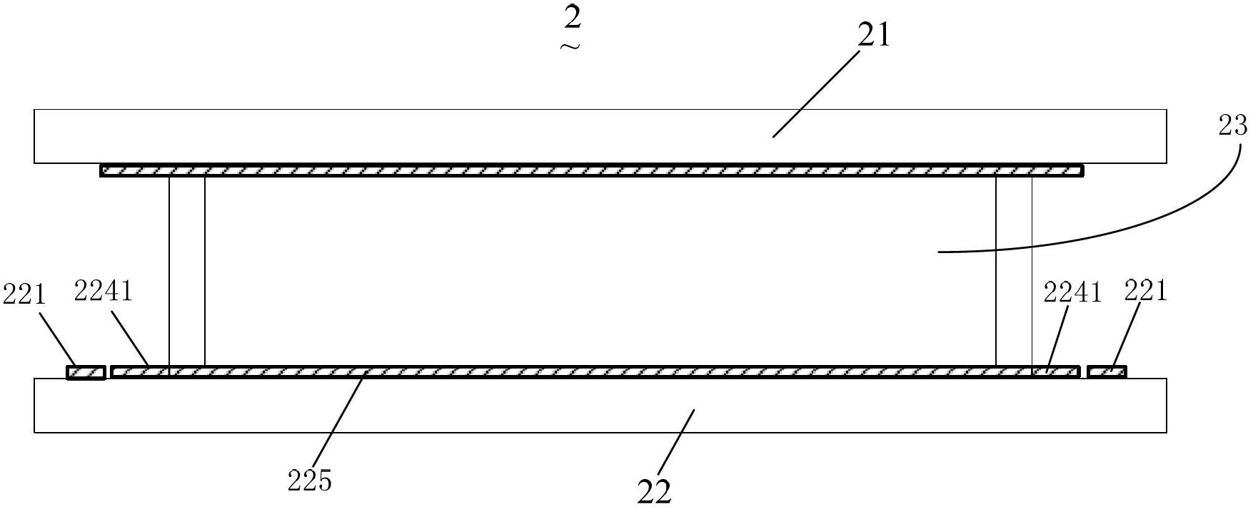
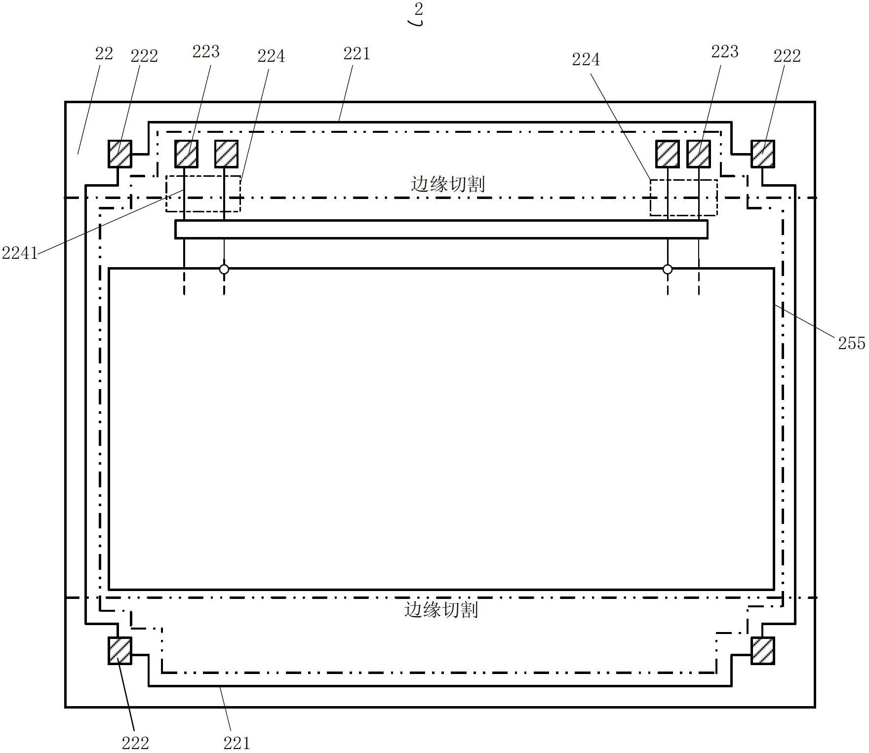
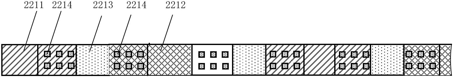
[0024] see figure 1 , figure 2 as well as image 3 , figure 1 is a schematic structural diagram of a liquid crystal display device in an embodiment of the present invention; figure 2 yes figure 1 A schematic diagram of the connection relationship of each line of the array substrate in the shown liquid crystal display device; image 3 yes figure 1 A schematic diagram of the connection relationship of each part of the reference line shown.

[0025] The liquid crystal display device 2 includes: a color filter substrate 21 , an array substrate 22 and a liquid crystal layer 23 sandwiched between the array substrate 22 and the color filter substrate 21 . The array substrate 22 includes a reference circuit 221 , a first test pad 222 , a second test pad 223 , an auxiliary circuit 224 and a semiconductor array circuit 225 . The semiconductor arra...


PUM


Abstract

The invention discloses a liquid crystal display device, an array substrate thereof, and a manufacturing method for the array substrate. The liquid crystal display device comprises the array substrate, a color filter substrate and a liquid crystal layer sandwiched between the array substrate and the color filter substrate. A voltage application circuit, a reference circuit and a first pad are arranged on the array substrate, wherein the reference circuit is adjacent to the voltage application circuit; and materials and manufacturing processes for the reference circuit and the voltage application circuit are the same. If the reference circuit is judged to have a defect, the voltage application circuit can be judged to probably have a defect by taking the defect of the reference circuit as a reference, and the array substrate can be specially controlled and repaired to reduce a defective rate.

Description

technical field [0001] The present invention relates to the technical field of LCD (Liquid Crystal Display, liquid crystal display), in particular to a liquid crystal display device, an array substrate and a method for manufacturing the array substrate. Background technique [0002] The prior art liquid crystal display generally includes: an array substrate, a color filter substrate, and a liquid crystal layer interposed between the array substrate and the color filter substrate. One of the liquid crystal display devices is provided with test pads, auxiliary circuits and semiconductor array circuits on the array substrate. The auxiliary circuit includes a pressurization circuit, and the pressurization circuit is respectively connected with the semiconductor array circuit and the test pad. [0003] PSVA (Polymer Stabilized Vertical Alignment, Polymer Stabilized Vertical Alignment technology) process is: cutting the edge of the color filter substrate to expose the test pad in...

Claims


Application Information

Patent Timeline
IPC IPC(8): G02F1/13G02F1/133G02F1/1362H01L21/77
CPCG02F1/1362G02F1/133G02F1/1345G02F1/13452G02F1/13454G02F1/136259G02F1/136254
Inventor 陈政鸿
Owner CHANGSHA HKC OPTOELECTRONICS CO LTD
Features
  • R&D
  • Intellectual Property
  • Life Sciences
  • Materials
  • Tech Scout
  • Unparalleled Data Quality
  • Higher Quality Content
  • 60% Fewer Hallucinations
Learn More