
GaN-based LED

A light-emitting diode, gallium nitride-based technology, applied in semiconductor devices, electrical components, circuits, etc., can solve the problems of excessive axial light emission from the front, uneven distribution of LED light emission, and small light emission angle, etc., to enhance the probability of light emission , Improve the uniformity of light distribution

Active Publication Date: 2012-10-03
ANHUI SANAN OPTOELECTRONICS CO LTD
View PDF3 Cites 21 Cited by
  • Summary
  • Abstract
  • Description
  • Claims
  • Application Information

AI Technical Summary

Problems solved by technology

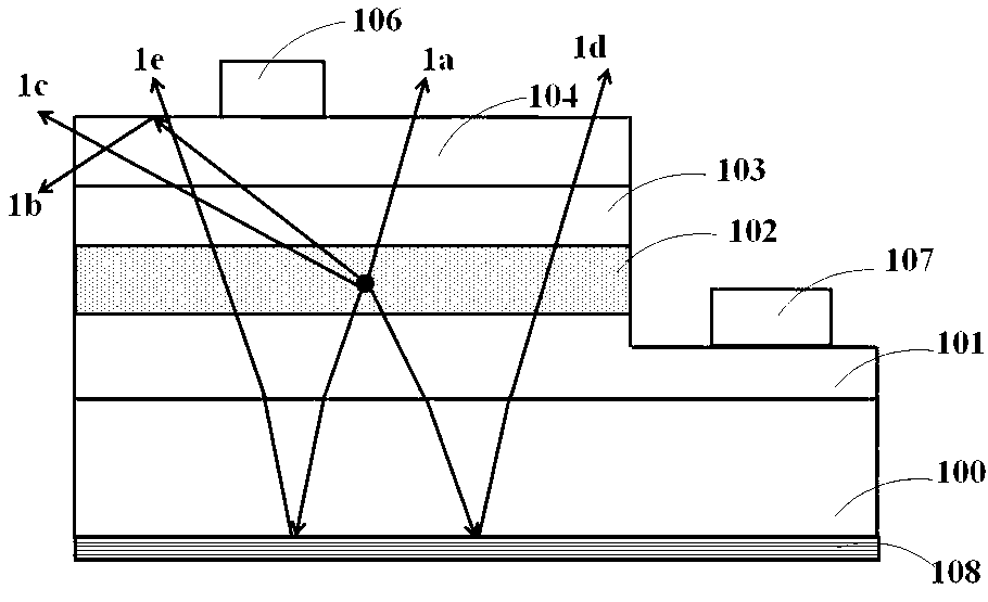
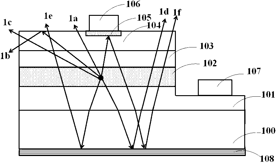
It can be seen that most of the light emitted from the light-emitting layer of the above two known front-mounted light-emitting diode structures is emitted from the front of the chip, while relatively little light is emitted from the side of the chip. Excessive light emission in the axial direction, insufficient heat dissipation, and small light emitting angle

Method used


Image

  • GaN-based LED
  • GaN-based LED
  • GaN-based LED

Examples


Embodiment 1

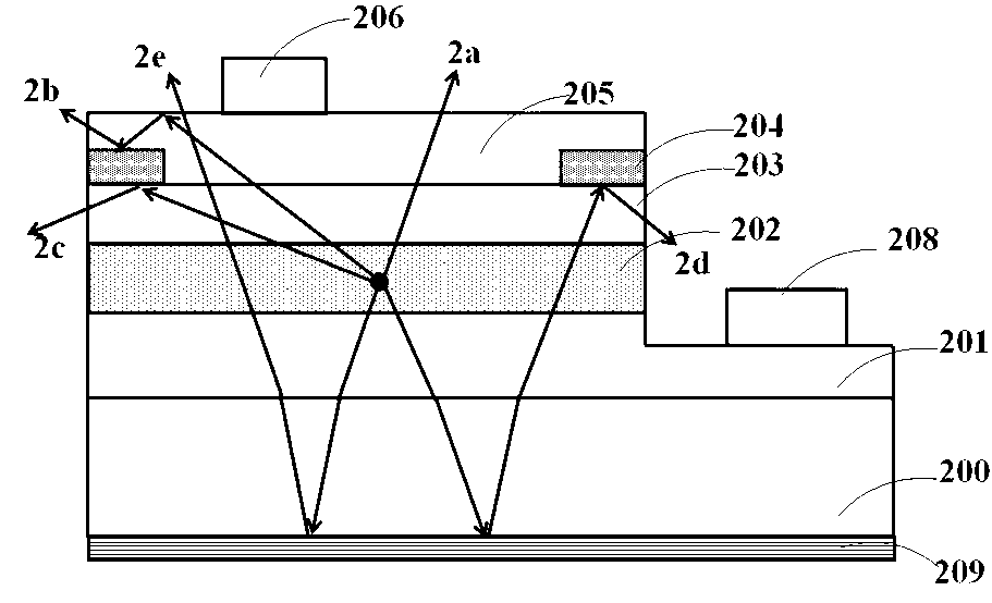
[0071] Such as image 3 and Figure 4 The gallium nitride-based high-brightness light-emitting diode shown includes: a sapphire substrate 200, an N-type layer 201, a light-emitting region 202, a P-type layer 203, a non-closed ring-shaped first reflective layer 204, and a current spreading layer 205 , P electrode 207, N electrode 208 and second reflective layer 209.

[0072] Specifically, the bottommost layer in the above light emitting diode structure is the sapphire substrate 200; the N-type layer 201 is formed on the sapphire substrate 200; the light-emitting region 202 is formed on the N-type layer 201; the P-type layer 203 is formed on the light-emitting region 202 The first reflective layer 204 is a distributed Bragg reflective layer, formed on the P-type layer 203 and distributed on the edge region of the P-type layer 203 away from the P-electrode, with a strip width of 15 microns and an area accounting for 10% of the light-emitting area of ​​the epitaxial layer About ...

Embodiment 2

[0075] Such as Figure 5 and Figure 6 The gallium nitride-based high-brightness light-emitting diode shown includes: a sapphire substrate 200, an N-type layer 201, a light-emitting region 202, a P-type layer 203, a closed-loop first reflective layer 204, a current spreading layer 205, The third reflective layer 206 , the P electrode 207 , the N electrode 208 and the second reflective layer 209 .

[0076] Specifically, the bottommost layer in the above light emitting diode structure is the sapphire substrate 200; the N-type layer 201 is formed on the sapphire substrate 200; the light-emitting region 202 is formed on the N-type layer 201; the P-type layer 203 is formed on the light-emitting region 202 . The first reflective layer 204 is a distributed Bragg reflective layer, formed on the P-type layer 203 and distributed in the edge region of the surface of the P-type layer 203 . The strip width of the first reflective layer is 20 microns, and its area accounts for about 25% ...

Embodiment 3

[0080] Compared with Embodiment 2, this embodiment discloses a gallium nitride-based high-brightness light-emitting diode with a vertical structure and a reflective layer structure. In this embodiment, Si is used as the substrate 200, and the N electrode 208 is formed on the back of the substrate, forming a vertical LED device structure. The third reflective layer is an omnidirectional reflective layer with a diameter of 70 microns, and the diameter of the third reflective layer 206 is smaller than that of the P electrode, which facilitates the contact and conduction between the P electrode and the current spreading layer 205 .

[0081] To sum up, the main design spirit of the reflective layer structure of the present invention lies in: (1) the first reflective layer can be in the form of a closed ring or an open ring; (2) the reflective layer with (ring) shape The edge region coincides with the edge region of the surface of the epitaxial layer. Through the reasonable design ...


PUM

PropertyMeasurementUnit
Diameteraaaaaaaaaa

Abstract

The invention relates to a GaN-based LED, which comprises a substrate, an epitaxial layer, a current extension layer and a P electrode, wherein the substrate is provided with a front surface and a back surface; the epitaxial layer is formed on the front surface of the substrate and comprises a P-type layer, a light-emitting region and an N-type layer from top to bottom in sequence; the current extension layer is formed on the P-type layer; and the P electrode is formed on the current extension layer. The GaN-based LED is characterized by further comprising a first reflecting layer and a second reflecting layer, wherein the first reflecting layer is positioned between the current extension layer and the epitaxial layer and is zonally distributed on a marginal area of the epitaxial layer; and the second reflecting layer is positioned on the back surface of the substrate. According to the invention, the zonal or annular first reflecting layer is arranged on the marginal area of the surface of the LED epitaxial layer, the probability of taking light from the side surface of the LED can be enhanced, namely, the proportion of light emitted from the light-emitting layer, which is emergent to the upper side to light emitted from the light-emitting layer, which is emergent to the side surface, is controlled, therefore the emergent light distribution uniformity of a chip is adjusted, and the nonuniform heat-radiation phenomenon is improved.

Description

technical field [0001] The invention relates to a gallium nitride-based light-emitting diode, in particular to a gallium nitride-based high-brightness light-emitting diode with a reflective layer. Background technique [0002] Light Emitting Diode (English for Light Emitting Diode, referred to as LED) is a semiconductor light emitting device made of the principle of P-N junction electroluminescence of semiconductors. LED has the advantages of no pollution, high brightness, low power consumption, long life, low working voltage, and easy miniaturization. Since the gallium nitride (GaN)-based LED was successfully developed in the 1990s, with the continuous progress of research, its luminous brightness has also been continuously improved, and its application fields have become wider and wider. As the efficiency of power GaN-based LEDs continues to increase, it will become an unstoppable trend to replace existing lighting sources with GaN-based LED semiconductor lamps. However,...

Claims


Application Information

Patent Timeline
IPC IPC(8): H01L33/10
CPCH01L33/46H01L33/10H01L33/14H01L33/32
Inventor 郑建森林素慧彭康伟洪灵愿尹灵峰
Owner ANHUI SANAN OPTOELECTRONICS CO LTD
Learn More