Full-automatic semiconductor wafer laser processing device and processing method thereof

A laser processing and semiconductor technology, which is applied in semiconductor/solid-state device manufacturing, laser welding equipment, metal processing equipment, etc., can solve the problem of inability to realize seamless connection of laser processing equipment, high fragmentation rate and defective rate, and affecting product quality, etc. problems, to achieve the effect of saving manual transfer steps, improving quality and avoiding pollution

Active Publication Date: 2014-08-13
HEFEI ZHICHANG PHOTOELECTRIC TECH
View PDF5 Cites 0 Cited by
  • Summary
  • Abstract
  • Description
  • Claims
  • Application Information

AI Technical Summary

Problems solved by technology

[0003] 1. Generally, two operators are required to operate one piece of equipment on average, resulting in waste of human resources and low efficiency
[0004] 2. Manual operation is prone to errors, resulting in a high rate of fragmentation and defective products
[0005] 3. Manual operation is easy to pollute the wafer and affect product quality
[0006] 4. Manual operation cannot realize the seamless connection between the laser processing equipment and the previous and subsequent processes

Method used


Image

  • Full-automatic semiconductor wafer laser processing device and processing method thereof
  • Full-automatic semiconductor wafer laser processing device and processing method thereof
  • Full-automatic semiconductor wafer laser processing device and processing method thereof

Examples


Embodiment Construction

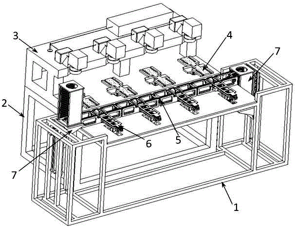
[0035] See figure 1 , a fully automatic semiconductor wafer laser processing device is composed of a front support 1, a rear support 2, a laser processing system 3, four rotating platforms 4, an automatic transmission system 5, and four automatic pick-up / placement devices opposite to the rotating platform 4 wafer system 6 and two wafer cassette lifting systems 7; laser processing system 3 and four rotating platforms 4 are all set on the rear support 2; The wafer magazine lifting system 7 is arranged on the front support 1, and two wafer magazine lifting systems 7 are respectively arranged at both ends of the automatic transmission system 5;

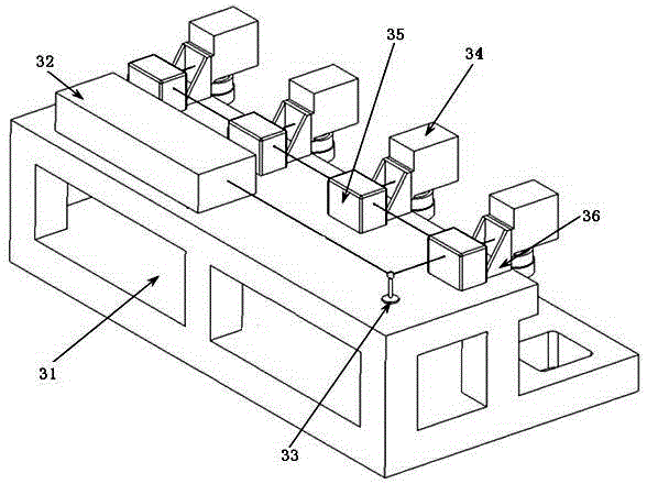
[0036] See figure 2 , the laser processing system 3 includes a two-layer stepped support platform 31, a laser 32, a reflector 33, four scanning galvanometers 34 opposite to the rotary platform 4, and four beam splitters and lasers that cooperate with each scanning galvanometer 34 respectively. Beam power real-time monitoring and adjust...


PUM


Abstract

The invention discloses a full-automatic semiconductor wafer laser processing device and a processing method thereof. The full-automatic semiconductor wafer laser processing device is composed of a front support, a rear support, a laser processing system, a plurality of rotating platforms, an automatic transportation system, a plurality of automatic wafer fetching / placing systems corresponding to the rotating platforms and two wafer box lifting systems, wherein the laser processing system and the plurality of rotating platforms are all arranged on the rear support; the automatic transportation system, the plurality of automatic wafer fetching / placing systems and the two wafer box lifting systems are all arranged on the front support; and the two wafer box lifting systems are respectively arranged at the two ends of the automatic transportation system. The full-automatic semiconductor wafer laser processing device employs an automatic feed system, an automatic discharge system and an automatic processing system for processing, and operators only need to switch on and off the related parts, therefore, the device is safe and simple to operate.

Description

technical field [0001] The invention relates to the field of semiconductor wafer production and manufacturing, in particular to a fully automatic semiconductor wafer laser processing device and a processing method thereof. Background technique [0002] In recent years, with the promotion and application of laser processing technology, laser processing equipment has been widely used in the field of semiconductor wafer manufacturing. Especially in the field of photovoltaic cells, the application of laser technology has greatly improved the production efficiency and quality of solar cells, and at the same time reduced the production and manufacturing costs of solar cells to a large extent. However, at present, most of the laser processing equipment for semiconductor wafers, including photovoltaic cells, still use a semi-automatic method of manual loading and unloading, which has the following shortcomings that urgently need to be improved: [0003] 1. Generally, two operators ...

Claims


Application Information

Patent Timeline
Patent Type & Authority Patents(China)
IPC IPC(8): B23K26/00B23K26/70H01L21/67B23K26/08
Inventor 翟骥吴周令
Owner HEFEI ZHICHANG PHOTOELECTRIC TECH
Why Eureka
Try Eureka