Driving circuit unit, gate driving circuit and display device

A gate drive circuit and drive circuit technology, applied in static indicators, instruments, etc., can solve the problems of increasing the rise time of the output signal pulse, increasing the total power consumption of the circuit, reducing the drive current, etc. The effect of widening the effective pulse width and reducing the total power consumption

Active Publication Date: 2012-10-10
PEKING UNIV SHENZHEN GRADUATE SCHOOL +1
View PDF2 Cites 57 Cited by
  • Summary
  • Abstract
  • Description
  • Claims
  • Application Information

AI Technical Summary

Problems solved by technology

I M will follow μ EF decreases, resulting in a decrease in the driving capability of the amorphous silicon TFT
Therefore M 2 The clock signal V MA A high level is coupled to the output node V MO When the driving current decreases, the rise time of the output signal pulse increases, which reduces the effective pulse width of the output signal used to drive the gate scan line; this will limit the application of the circuit in low temperature applications
[0009] Second, power consumption
So when the dynamic power consumption of the gate drive circuit increases, the total power consumption of the circuit will also increase significantly
In the display of mobile devices, the increase of power consumption will reduce the battery life, resulting in insufficient battery life of mobile devices

Method used


Image

  • Driving circuit unit, gate driving circuit and display device
  • Driving circuit unit, gate driving circuit and display device
  • Driving circuit unit, gate driving circuit and display device

Examples


Embodiment 1

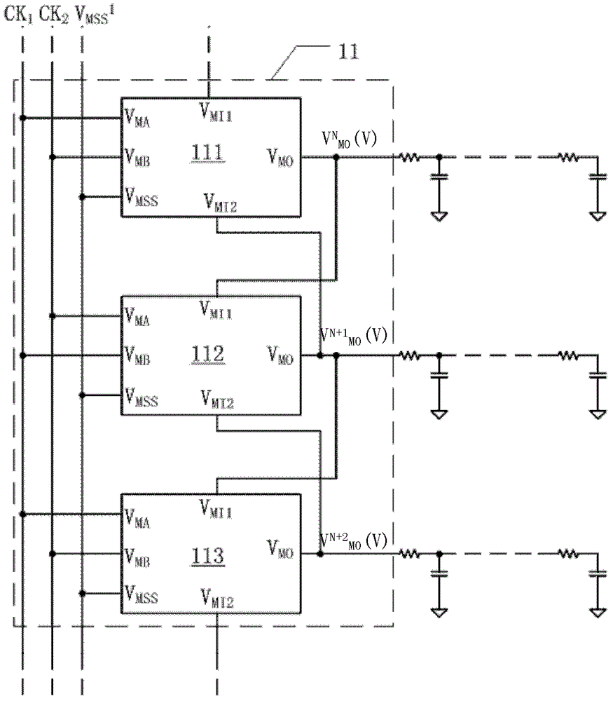
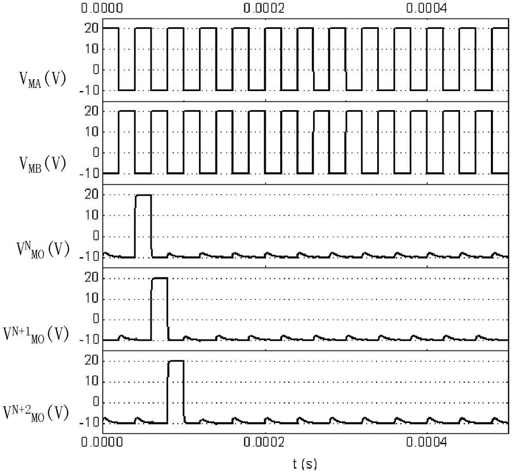
[0055] Such as Figure 7 As shown, the drive circuit unit includes five modules: an input module 71 , a drive module 72 , a discharge module 73 , a clock feedthrough suppression module 74 and a low level maintenance module 75 . Figure 8 is the timing diagram of the drive circuit unit. Detailed description below Figure 7 The operation of the circuit shown.

[0056] The first input signal V I1 is the output signal V of the N-1th stage drive circuit unit N-1 O , the second input signal V I2 is the output signal V of the N+1th level drive circuit unit N+1 O , the third input signal V I3 is the output signal V of the N+2th stage drive circuit unit N+2 O . Among them, the N-1th stage output signal V N-1 O , Nth stage output signal V N O , output signal V of stage N+1 N+1 O and output signal V of the N+2 stage N+2 O Both are pulse signals with a pulse width of T / 2, and they are overlapped sequentially for a time of T / 4. The first clock signal V A , the third cl...

Embodiment 2

[0078] Figure 9 Shown is the structure of the drive circuit unit of the second embodiment, including an input module 91, a drive module 92, a discharge module 93, a clock feedthrough suppression module 94 and a low level maintenance module 95, wherein the drive module 92, the discharge module 93, The clock feedthrough suppression module 94 and the low-level maintenance module 95 still use the circuit modules described in Embodiment 1, which will not be repeated here.

[0079] Such as Figure 9 As shown, the input module circuit unit 91 includes a first transistor T 1 , the fourth input signal V I4 , where the fourth input signal V I4 Input the output signal V of the N-2 drive circuit unit N-2 O . Figure 9 The timing diagram of the drive circuit unit is shown in Figure 10 shown. This embodiment and embodiment one (namely Figure 7 The difference in the circuit structure of the shown drive circuit unit) is: the first transistor T in the input module 91 1 The gate an...

Embodiment 3

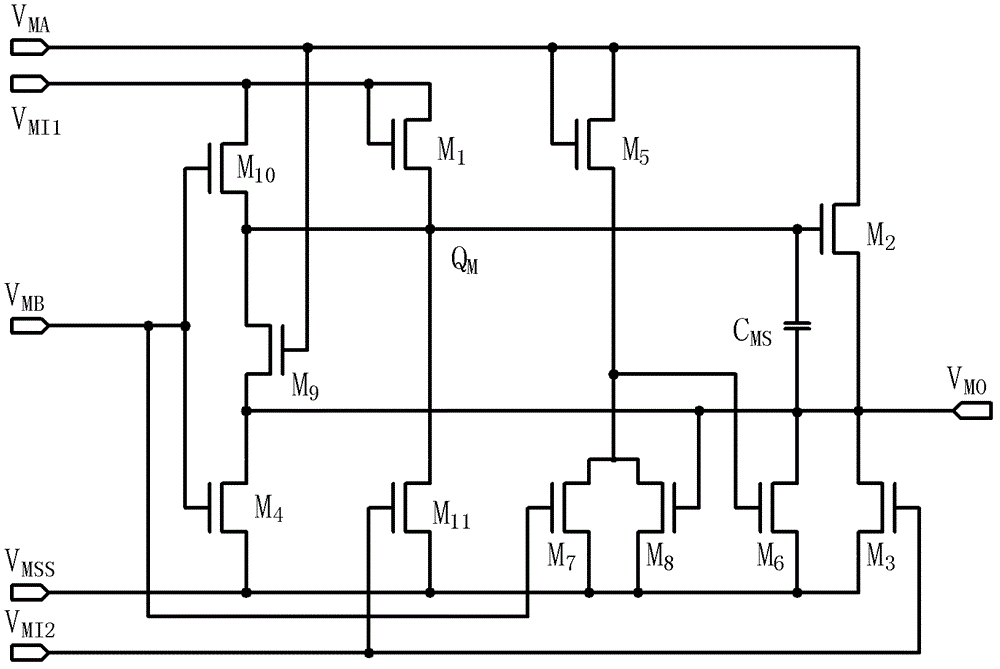
[0081] Figure 11 Shown is the structure of the drive circuit unit of the third embodiment, including an input module 111, a drive module 112, a discharge module 113, a clock feedthrough suppression module 114 and a low level maintenance module 115, wherein the input module 111, the drive module 112, The clock feedthrough suppression module 114 and the low-level maintenance module 115 still use the circuit modules described in Embodiment 1, which will not be repeated here.

[0082] Such as Figure 11 As shown, the unit circuit of the discharge module 113 includes: a third transistor T 3 , two input signals (the second clock signal V B , the third input signal V I3 ). Figure 11 The timing diagram of the drive circuit unit is shown in Figure 12 shown. Figure 12 The timing sequence of the driving circuit unit shown is similar to that of the second embodiment, and will not be repeated here. Compared with the second embodiment, the advantage of this embodiment is: because...


PUM


Abstract

The invention relates to a gate driving circuit and a display device. The gate driving circuit comprises multiple levels of driving circuit units connected in series. Each level of units comprises an inputting module for providing threshold voltage of a driving module, a driving module for responding to the threshold voltage and for sending a first clock signal to a signal outputting interface, a discharging module for responding to an output signal or a clock signal of an adjacent level and for coupling a control terminal of the driving module to a first voltage source, a clock feedthrough inhibiting module for stablizing the potential of the control terminal of the driving module under the control of the clock signal and the output signal of the adjacent level, and a low level maintaining module for stablizing the output signal at the potential of the first voltage source under the control of the clock signal. The driving circuit unit, gate driving circuit and display device provided by the invention employ single driving tube to realize the fast pull-up and pull-down of the output signal with sequential coordination, reducing the delay time of the rise and fall of the output signal at a low temperature, and employs the clock feedthrough inhibiting module to stablize the gate potential of the driving tube, reducing the corresponding dynamic power consumption.

Description

technical field [0001] The present invention relates to the field of display technology, in particular to a display device and a gate driving circuit adopted therefor. Background technique [0002] Thin film transistor (TFT) flat panel display (FPD, Flat Panel Display) technology is the mainstream of display technology today. Among them, the integrated gate drive circuit is a new technology emerging in the development of FPD technology; the advantage of integrating the gate drive circuit on the display substrate (such as glass) is that the number of peripheral drive chips and its sealing process are reduced. , enabling the realization of light-weight, thin-thick and symmetrical narrow-frame panels, the liquid crystal module is more compact, and the mechanical and electrical reliability of the display device is enhanced, and it is possible to simplify the gate-source drive circuit and improve the resolution of the display panel rate, and increase the possibility of realizing...

Claims


Application Information

Patent Timeline
Patent Type & Authority Applications(China)
IPC IPC(8): G09G3/36
Inventor 张盛东郑灿廖聪维陈韬刘晓明戴文君钟德镇简庭宪
Owner PEKING UNIV SHENZHEN GRADUATE SCHOOL
Why Eureka
Try Eureka