Overlay method for nano-scale components

A nanoscale and component technology, applied in the field of nanoscale component preparation, can solve problems such as slow manufacturing progress, limited process development, easy collapse of photoresist, etc., and achieve the effect of large resolution

Active Publication Date: 2012-10-17
INST OF MICROELECTRONICS CHINESE ACAD OF SCI
View PDF4 Cites 3 Cited by
  • Summary
  • Abstract
  • Description
  • Claims
  • Application Information

AI Technical Summary

Problems solved by technology

However, the manufacture of nano-scale components is progressing very slowly. The reason is that the influence of surface tension makes the thin-line photoresist very easy to collapse, thus limiting the further development of its technology.

Method used


Image

  • Overlay method for nano-scale components
  • Overlay method for nano-scale components
  • Overlay method for nano-scale components

Examples


Embodiment Construction

[0023] In order to make the object, technical solution and advantages of the present invention clearer, the present invention will be described in further detail below in conjunction with specific embodiments and with reference to the accompanying drawings.

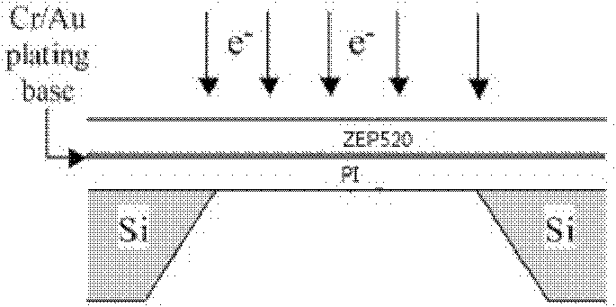
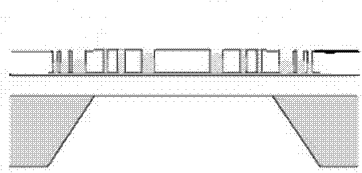
[0024] Such as Figure 8 as shown, Figure 8 It is a schematic diagram of layout making principle provided by the present invention. According to this schematic diagram, the final figure = figure A and figure B are engraved together. The second ring is the zone plate figure made by figure A, and the third ring is the zone plate figure made by figure B, and they form the final zone plate figure after overlaying. The zone plate rings of this graph are the first ring of graph A, the first ring of graph B, the second ring of graph A, the second ring of graph B, ... from inside to outside.

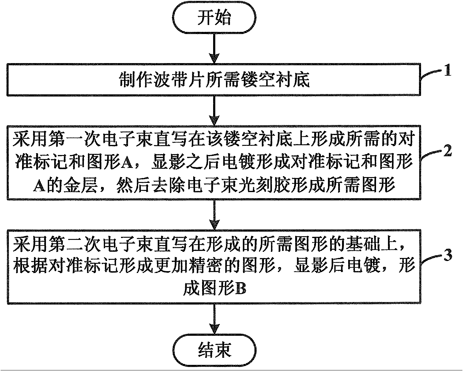
[0025] based on Figure 8 The principle shown, figure 1 The flow chart of the method for overlaying nanoscale components provided by...


PUM


Abstract

The invention discloses an overlay method for nano-scale components. The method comprises the steps: making a zone plate required hollow substrate, employing electron-beam direct writing for the first time to form a required alignment mark and a pattern A on the hollow substrate, forming a gold layer of the alignment mark and the pattern A by electroplating after developing, removing electron beam photoresist to form the required patterns afterwards, employing the electron-beam direct writing for the second time on the basis of the required patterns formed to form more precise patterns according to the alignment mark, and electroplating after developing to form a pattern B. Compared with the components made by a conventional nanometer manufacturing process, the components made by the overlay process method for nano-scale components provided by the invention have greater resolution, denser lines, and more broad prospects in the application aspect of high-precision components.

Description

technical field [0001] The invention relates to the technical field of preparation of nanoscale components, in particular to an overlay process method for nanoscale components. Background technique [0002] As we all know, with the continuous development of nanofabrication technology, the required components become more and more precise, such as the width of the outermost ring of the zone plate, which is an important factor affecting the resolution of the zone plate. However, the manufacture of nanoscale components is progressing very slowly. The reason is that the influence of surface tension makes the photoresist of thin lines collapse easily, thus limiting the further development of its technology. [0003] For thinner and thinner line widths, the process requirements are getting higher and higher, the difficulty is getting more and more difficult, and the possibility of realization is very small. The invention adopts a two-step photolithography manufacturing process to ...

Claims


Application Information

Patent Timeline
Patent Type & Authority Applications(China)
IPC IPC(8): G03F7/20G03F9/00
Inventor 谢常青方磊朱效立李冬梅刘明
Owner INST OF MICROELECTRONICS CHINESE ACAD OF SCI
Why Eureka
Try Eureka