Substrate processing method

A substrate processing device and processing chamber technology, which is applied in the direction of discharge tubes, electrical components, plasma, etc., can solve the problems of poor controllability of etching processing and achieve the effect of improving processing controllability

Active Publication Date: 2012-10-17
TOKYO ELECTRON LTD
View PDF5 Cites 2 Cited by
  • Summary
  • Abstract
  • Description
  • Claims
  • Application Information

AI Technical Summary

Problems solved by technology

That is, there is a problem that the process controllability of etching is not so good when using LF high-frequency voltage to generate a bias voltage on the susceptor

Method used


Image

  • Substrate processing method
  • Substrate processing method
  • Substrate processing method

Examples


Embodiment Construction

[0039] Hereinafter, embodiments of the present invention will be described with reference to the drawings.

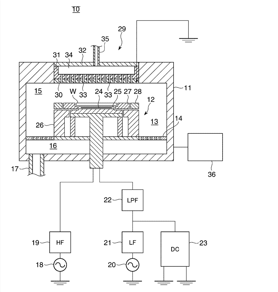
[0040] figure 1 It is a cross-sectional view schematically showing the structure of the substrate processing apparatus of this embodiment. This substrate processing apparatus performs plasma processing on a wafer for a semiconductor device (hereinafter referred to simply as a "wafer") as a substrate.

[0041] exist figure 1 Among them, the substrate processing apparatus 10 has, for example, a chamber 11 for accommodating a wafer W having a diameter of 300 mm, and a columnar susceptor 12 (mounting table) on which the wafer W is placed on the upper surface is arranged in the chamber 11 . In the substrate processing apparatus 10 , the side exhaust passage 13 is formed by the inner side wall of the chamber 11 and the side surface of the susceptor 12 . An exhaust plate 14 is arranged in the middle of the side exhaust passage 13 .

[0042] The exhaust plate 14 is a plat...


PUM


Abstract

A substrate processing apparatus capable of improving a processing controllability in an etching process is provided. The substrate processing apparatus (10) includes a depressurized processing room (11); a susceptor (12) that is provided in the processing room (11) and configured to mount a wafer (W) thereon; a HF high frequency power supply (18) configured to apply a high frequency voltage for plasma generation to the susceptor (12); a LF high frequency power supply (20) configured to apply a high frequency voltage for a bias voltage generation to the susceptor (12); and a DC voltage applying unit (23) configured to apply a DC voltage of a rectangle-shaped wave to the susceptor (12).

Description

technical field [0001] The present invention relates to a substrate processing method for performing predetermined processing on a substrate using plasma. Background technique [0002] A substrate processing apparatus for performing predetermined plasma processing on a semiconductor wafer (hereinafter referred to as "wafer") as a substrate using plasma, comprising: a depressurized processing chamber; a mounting table arranged in the processing chamber; and a mounting table connected to the processing chamber 1. An HF high-frequency power supply that applies a relatively high-frequency high-frequency voltage (hereinafter referred to as "HF (High Frequency, high frequency) high-frequency voltage") to the base as the mounting table; An LF high-frequency power supply that applies a relatively low-frequency high-frequency voltage (hereinafter referred to as "LF (Low Frequency, low frequency) high-frequency voltage"). [0003] The HF high-frequency voltage excites the processing ...

Claims


Application Information

Patent Timeline
Patent Type & Authority Applications(China)
IPC IPC(8): H01J37/32
CPCH01J37/32706H01J37/32091H01J37/32165H01J37/32H01J37/32082H01J37/32366H01J37/32642H01J37/32697H01J37/32724H05H1/46H01L21/3065H01J2237/327
Inventor 桧森慎司山田纪和大瀬刚
Owner TOKYO ELECTRON LTD
Why Eureka
Try Eureka