Optical proximity correction method

An optical proximity correction and exposure technology, which is applied in the semiconductor field, can solve the problems of long cycle time and increase the production cost of semiconductor foundries, and achieve the effect of saving process time

Active Publication Date: 2012-10-31
SEMICON MFG INT (SHANGHAI) CORP
View PDF6 Cites 11 Cited by
  • Summary
  • Abstract
  • Description
  • Claims
  • Application Information

AI Technical Summary

Problems solved by technology

[0007] In the above-mentioned existing model-based method for verifying optical proximity correction, once a weakness is found, it is necessary to verify the entire pattern to be exposed under all different verification conditions, and it is necessary to perform an optical proximity correction process menu (OPC recipe) is optimized, which makes the cycle time of the entire optical proximity correction process very long, increasing the production cost of the semiconductor foundry

Method used


Image

  • Optical proximity correction method
  • Optical proximity correction method
  • Optical proximity correction method

Examples


Embodiment Construction

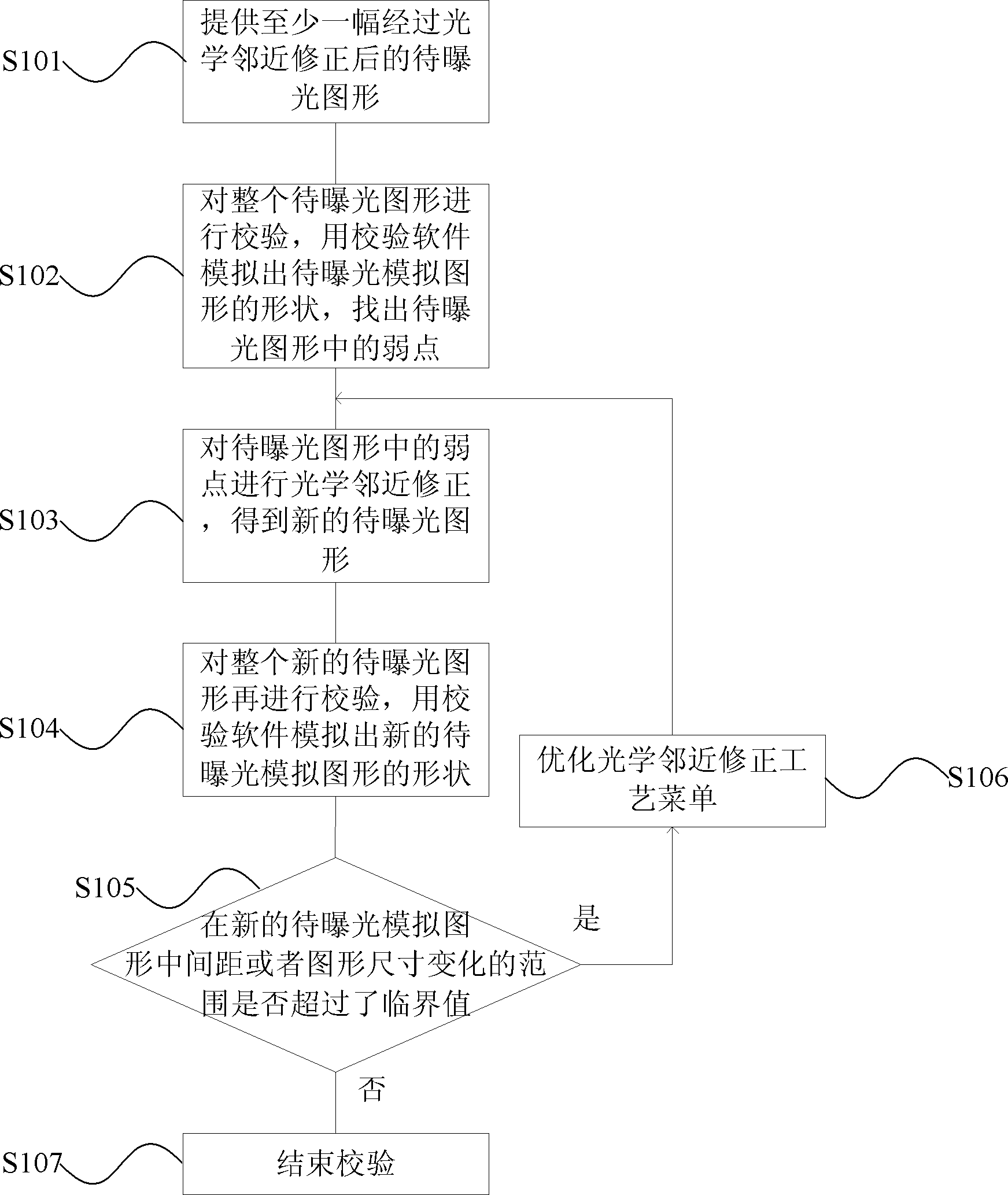
[0025] The inventor found that the optical proximity correction parameters of the optical proximity correction program need to be adjusted several times during the optical proximity correction process, which makes the optical proximity correction take a long time, and it is impossible to verify whether the optical proximity correction parameters are optimal, so that the optical proximity correction The effect of the proximity correction is not necessarily the optimal effect, and, with the reduction of the semiconductor feature size, the adjustment of the optical proximity correction parameters is more frequent, thereby further increasing the time of the optical proximity correction.

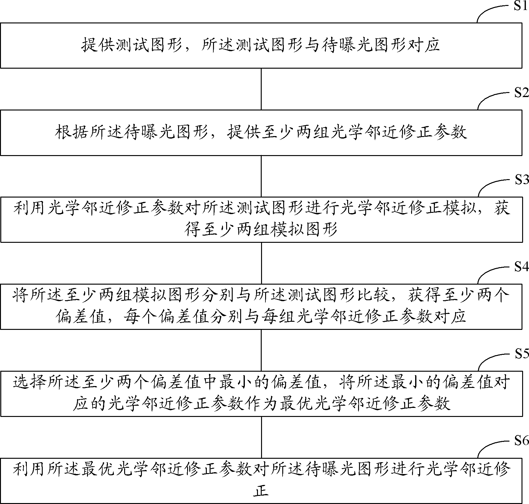
[0026] The inventor considers that if the optimal optical proximity correction parameters can be determined before the optical proximity correction is performed on the graphics to be exposed, so as to use the optimal optical proximity correction parameters to perform optical proximity correction on...


PUM


Abstract

An embodiment of the invention provides an optical proximity correction method which includes: providing a testing picture which corresponds to a picture to be exposed; providing at least two groups of optical proximity correction parameters according to the picture to be exposed; using the optical proximity correction parameters to perform optical proximity correction simulation to the testing picture so as to obtain at least two groups of simulated pictures; comparing the two groups of the simulated pictures with the testing picture to obtain at least two deviation values, with each deviation value corresponding to each group of the optical proximity correction parameter respectively; selecting the minimum deviation value and using the optical proximity correction parameter corresponding to the minimum deviation value as optimal optical proximity correction parameter; and performing optical proximity correction to the picture to be exposed according to the optimal optical proximity correction parameter. By the method, cycle time of the optical proximity correction is reduced, and production cost of semiconductor foundries is saved.

Description

technical field [0001] The invention relates to the technical field of semiconductors, in particular to an optical proximity correction method. Background technique [0002] In the semiconductor manufacturing process, in order to overcome a series of optical proximity effects (Optical Proximity Effect, OPE) brought about by the reduction of the critical dimension (Critical Dimension, CD), the industry has adopted a lot of resolution enhancement technology (Resolution Enhancement Technology, RET ), including technologies such as optical proximity correction, phase shifting mask (Phase Shifting Mask, PSM) and off-axis illumination (Off Axis Illumination, OAI). [0003] The model-based optical proximity correction (MBOPC) method is a kind of optical proximity correction method, also known as the simulated optical proximity correction method. It mainly compares the simulated graphics to be exposed with the target graphics, and establishes the correction mode of the graphics to b...

Claims


Application Information

Patent Timeline
Patent Type & Authority Applications(China)
IPC IPC(8): G03F7/20
Inventor 杨青刘娟
Owner SEMICON MFG INT (SHANGHAI) CORP
Why Eureka
Try Eureka