Layout structure of capacitive touch panel

A touch panel and layout structure technology, applied in the direction of electrical digital data processing, input/output process of data processing, instruments, etc., can solve the problems of increasing costs, reduce manufacturing costs, simplify the number of masks and process complexity Effect

Active Publication Date: 2012-10-31
NOVATEK MICROELECTRONICS CORP
View PDF2 Cites 4 Cited by
  • Summary
  • Abstract
  • Description
  • Claims
  • Application Information

AI Technical Summary

Problems solved by technology

However, the double conductive layer structure of the traditional mutual capacitive touch panel increases the cost due to the configuration of the above double conductive layer

Method used


Image

  • Layout structure of capacitive touch panel
  • Layout structure of capacitive touch panel
  • Layout structure of capacitive touch panel

Examples


Embodiment Construction

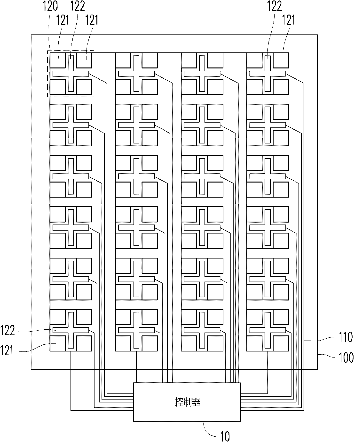
[0020] figure 1 It is a schematic diagram illustrating the layout structure of a capacitive touch panel 100 according to an embodiment of the present invention. The layout structure of the capacitive touch panel 100 includes a plurality of electrical paths 110 and a plurality of first touch units (touch units, such as figure 1 Shown touch unit 120). For the implementation of other touch units in the capacitive touch panel 100 , reference may be made to the related description of the touch unit 120 . In this embodiment, the substrate can be made of polycarbonate (Polycarbonate, PC), polyethylene (Polyethylene, PE), polyethylene terephthalate (polyethylene terephthalate, PET), polymethyl methacrylate (PolyMethyl MethAcrylate, PMMA) or transparent materials such as glass substrates. The electrical path 110 and the first touch unit 120 can be made of any light-transmitting conductive material, such as nanometer indium-tin oxide (ITO) and the like.

[0021] Each first touch uni...


PUM


Abstract

The invention discloses a layout structure of a capacitive touch panel, which comprises a plurality of electrical paths and a plurality of touch units, wherein the touch units respectively comprise at least one receiving electrode and at least one driving electrode; the receiving electrodes and the driving electrodes are allocated in the same conducting layer; the receiving electrodes and the driving electrodes are insulated with each other; the receiving electrodes are connected to a controller by different electrical paths, and the driving electrodes are electrically connected with each other. According to the invention, the light cover quantity and process complexity are simplified, and the manufacturing cost is further lowered.

Description

technical field [0001] The present invention relates to a touch panel, in particular to a layout structure of a capacitive touch panel. Background technique [0002] The layout structure of traditional mutual capacitance touch panels is mostly a double conductive layer structure. Wherein, the driving electrode is configured in one of the double conductive layers, and the receiving electrode is configured in the other conductive layer of the double conductive layer. However, the double conductive layer structure of the traditional mutual capacitive touch panel increases the cost due to the configuration of the above double conductive layer. Contents of the invention [0003] The invention provides a layout structure of a capacitive touch panel, which can be implemented in a single conductive layer to reduce costs. [0004] Embodiments of the present invention provide a layout structure of a capacitive touch panel. The layout structure includes a plurality of electrical p...

Claims


Application Information

Patent Timeline
IPC IPC(8): G06F3/044
Inventor 赖志章
Owner NOVATEK MICROELECTRONICS CORP
Why Eureka
Try Eureka